Having spent the last 30 years in semiconductor manufacturing, eight years of this living and working in Asia, it is both exciting and unsettling to see renewed political interest in the revitalization of this industry in the United States. Gone are the days of ‘It doesn’t make any difference whether a country makes computer chips or potato chips!’ usually attributed to Michael J. Boskin, who served on President George H.W. Bush’s economic council. Chips of the computer variety are now a national security and economic priority.
But the successful return of the US to semiconductor manufacturing prominence is by no means a sure bet. Bipartisan support for the CHIPS for America Act is highly encouraging, but funding alone may not solve the systemic issues that have driven the disproportionate growth of overseas manufacturing in the semiconductor industry.
The Semiconductor Value Chain
Six of the top ten semiconductor companies in 2018 had US headquarters. These are Intel, Micron, Broadcom, Qualcomm, Texas Instruments (TI), and nVidia. Intel, Micron, and TI are Integrated Device Manufacturers, or IDM’s. This means that they produce the majority of their products in factories that they own and operate themselves. These factories may be located in the United States or abroad but are typically a combination of both. Broadcom, nVidia and Qualcomm are fabless semiconductor companies. They design and market semiconductor chips but rely on wafer foundries and Outsourced Semiconductor Assembly and Test (OSAT) service providers to manufacture their designs.
Intel produces CPU and GPU devices. Micron produces memory devices. These are both high-volume relatively low mix products that demand continuous investment in capital assets to increase performance. TI primarily produces analog and embedded processor devices. These devices are less capital intensive because product life cycles are longer and new designs can be implemented without replacing entire manufacturing lines.
Broadcom, Qualcomm, and nVidia are a different breed of semiconductor company known as fabless suppliers. They don’t own or operate their own manufacturing facilities. They source integrated circuits in wafer form from merchant suppliers known as wafer foundries and have these chips diced, packaged, and tested OSAT companies. While Globalfoundries and Samsung have wafer fabrication facilities in the US and TSMC has announced plans to build a facility in Arizona, the vast majority of fabless semiconductor manufacturing is done in Asia. There are no large OSAT factories in the US. Semiconductor packaging and test is done predominantly in Asia.
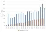
As shown in Figure 1 below, the fabless segment of the global semiconductor industry has grown from 7% of the total industry in 1999 to 30% in 2019. This represents a 13% compounded annual growth rate versus 4% for the IDM segment of the market. The volatility of the IDM portion of the market is also noticeably higher. This is primarily driven by the large revenue contribution of the memory devices and the fluctuation in the pricing of these products that results from frequent cycles of under and over supply conditions as competitors seek to generate cash to offset the large capital expenditures required to keep their factories at the leading edge.
Figure 1 (sourced from Statistica)
Intel, Micron, and TI all produce a significant portion of their semiconductor wafers in the United states but for the most part they ship these wafers to Asia for package assembly and final test. Why is this?
Package assembly and test moved to Asia beginning in the late 1960’s. At this time, these operations were highly manual and moving to Asia offered immediate labor costs savings. Times have changed though. Modern assembly process tools are now fully automated and direct labor typically represents only than 10% to 15% of manufacturing cost. While not as capital intensive as leading-edge wafer fabrication, package assembly and test does require continuous investment to support the higher levels of functional integration found in portable devices such as mobile phones as well as high-performance computing for cloud processing.
The OSAT business is highly competitive and gross margins are typically in the range of 20%. Asian manufactures have spent the last 50 years figuring out how to run these very lean businesses. It is difficult to make money in this business. Capital investments must be made without firm order volume. Larger OSAT’s run thousands of different part numbers in their giant factories at the same time. New product introductions are released continuously. Production ramps for hot new consumer products can be incredibly fast going from engineering level production to millions of units per week in less than a month. It is not a business for the faint of heart.
Why is the Merchant Supply Chain for Semiconductors Critical?
While the OSAT industry’s initial move to Asia was to reduce labor costs, the wafer foundry industry’s geographical concentration in Asia has a different history. As the cost of building a leading-edge wafer fab increased from a few hundred million dollars to over twelve billion dollars today, fewer companies had the financial resources to develop their own manufacturing technology and construct their own fabs. Companies with a dominant market position in a specific family of devices with predictable market demand could make these investments but smaller more specialized companies could not. By combining business from many smaller fabless design companies into a common factory and facilitating the ecosystem through internally developed and third-party IP blocks, TSMC created a unique solution that enabled the tremendous growth of the fabless segment of the market. Now many of the largest device companies in the world use wafer foundries and OSAT’s to do all their manufacturing.
This model benefits end-users as well. System designers can work with fabless suppliers to source chips without needing to reach the economic scale to support a dedicated factory. More design companies increase the variety of available chips and better align designs to a large variety of end use case.
This situation also creates a dilemma for the US defense industry whose volumes are not typically large but often require leading-edge manufacturing solutions.
What do Manufacturers in Taiwan know that US Manufacturers don’t?
Taiwan is now clearly the leader in semiconductor manufacturing with the worlds’ largest wafer fab (TSMC) and OSAT (ASE) headquartered there. Both companies do most of their manufacturing in Taiwan as well and have established highly competitive practices and a highly efficient ecosystem to keep their facilities running in a reliable and cost-effective manner.
Wafer fabrication can consist of more than 2000 process steps at the leading edge. To produce a device that functions properly, each of these process steps must be precisely controlled. While historically the packaging portion of the manufacturing process has been far less complex, increases in the functional density of end products such as smart phones and performance requirements of cloud computing have pushed packaging technology advances rapidly in recent years.
When many different products are built in the same line as in the case in wafer foundry or OSAT, the challenges intensify immensely. Product Lifecycle Management (PLM) and New Product Introduction (NPI) processes must be rigorously controlled. New products are often run on a single set of tools under engineering supervision. It can be months between the initial qualification of a new device and a subsequent ramp to high volume manufacturing. These ramps can be sudden and manufacturers must make sure that process recipes developed during NPI are followed precisely. The cost of a delay in the ramp of a new product can cause massive losses in revenue and market share for customers. Driven by a continuous flow of new products, merchant manufacturers in Taiwan have been very successful at developing their PLM and NPI processes. While these techniques can certainly be developed in other regions, the institutional knowledge these organizations have gained over decades of managing these complex requirements are invaluable and create a significant barrier to entry.
Manufacturers in Taiwan manage these complex process flows and PLM and NPI requirements while maintaining an unrelenting focus on costs. This pressure has created a large and complex ecosystem of smaller suppliers in Taiwan who make replacement parts and consumables at considerably lower prices than the Original Equipment Manufacturers (OEM’s). These suppliers compete relentlessly against each other while in turn driving down their own costs and raising productivity and quality. Over time, more and more complex components have been sourced from this domestic market saving Taiwan’s semiconductor manufacturers hundreds of millions of dollars on an annual basis.
What can the US Government and US Companies do to Create a Vibrant Domestic Semiconductor Manufacturing Industry
Passage of the CHIPS for America act is a vital first step, however it is important that the money be used in a way that promotes development of a sustainable domestic manufacturing ecosystem. Simply offsetting the existing cost differential between US and Asia manufacturing will have a temporary impact at best. The systemic differences between these markets must be addressed to ensure a long-term successful transformation of domestic semiconductor manufacturing.
Intense focus must be placed on understanding the root causes of the current imbalance between US and Asia manufacturing and funds directed in a way that overcomes these causes. The US should seek to create an ecosystem to support domestic merchant manufacturing that will enable fabless semiconductor companies to build their leading-edge products cost effectively and reliably in the US in domestic foundries and OSAT’s. This will provide the most benefits to both the commercial and defense industries.
A few specific actions are required to make this achievable.
First, eliminate the tax incentive to manufacture overseas. This is a no brainer. While fixing the loopholes that allow semiconductor companies who manufacture overseas to pay less tax seems attractive, the impact of such a decision needs to be weighed against the realities of the global competitive environment. Raising costs for US devices companies through higher taxes will benefit their international competitors. Better yet, allow domestic manufactures to enjoy the same tax benefits they see manufacturing overseas when building parts domestically.
Second, address the gaps in domain knowledge between US and Taiwan manufacturers. US IDM’s and foundries are not necessarily the experts on operating high volume, low cost foundries. There are no large US OSAT’s. Domestic manufacturing models and business processes have not developed in the same way as Taiwan over the last 20 years. The international transfer of manufacturing domain knowledge has fueled international growth in many industries. In the past, much of this domain knowledge transfer was from the US to Asia. In this case, the opposite is needed.
Third, build an entire ecosystem for semiconductor manufacturing and encourage private investment in the same. Scale is very important in wafer fabrication and packaging and test but a diverse ecosystem of materials, spare parts, and consumable materials are also necessary to achieve cost parity. Subsidize smaller manufacturers and machine shops to invest in the tools and development activities needed to support the semiconductor manufacturing industry. Make sure that third-party IP developers have incentive to make designs using domestic foundry design rules.
Forth, make sure manufacturers feel the competition and develop the ability to compete. This will not happen overnight but needs to be the end goal. Create incentives for manufacturers to operate with a dire sense of urgency. Make sure they ‘sweat the assets’ by pushing their capital asset productivity to at least the levels currently achievable in Taiwan. Give them aggressive but achievable cost targets to drive them to global competitiveness so that when government funding stops, they can compete in a global market.
Fifth, keep tight track of the CHIPS for America money and how it is used. It is surprisingly easy to destroy billions of dollars of capital in the semiconductor industry. Make sure end users have incentives to invest time and money in the qualification of domestic suppliers. Track progress and make sure that domestic manufacturers make continuous progress of yield, quality, cycle time, and cost. They won’t close the gap immediately, but they should be able to make continuous progress.
Conclusions
Semiconductor devices enable our interconnected world. While the US is a leader in semiconductor design, manufacturing equipment, and process technology, it lacks a vibrant semiconductor manufacturing sector, particularly for the vital fabless semiconductor segment of the industry. Recent events have prompted renewed public interest in a revitalized domestic semiconductor manufacturing industry. Public money can help promote the industry but money alone without proper allocation, management, and focus will not resolve the systemic issues that currently limit the ability of private enterprise to profitably compete in this market.