webinar banner AI 2026 v2

The Future of Chip Design with the Cadence iSpatial Flow

The Future of Chip Design with the Cadence iSpatial Flow
by Mike Gianfagna on 07-06-2020 at 10:00 am

Screen Shot 2020 06 20 at 2.30.57 PM

A few months ago, I wrote about the announcement of a new digital full flow from Cadence. In that piece, I focused on the machine learning (ML) aspects of the new tool. I had covered a discussion with Cadence’s Paul Cunningham a week before that explored ML in Cadence products, so it was timely to dive into a real-world example of the strategy Paul described. Since then, I also covered a position paper from Cadence on Intelligent System Design, which provides more details on advanced technology and ML for EDA.

The new digital full flow from Cadence is called iSpatial. Beyond ML, it also features unified placement and physical optimization engines that Cadence describes as an industry first. That’s a lot of integrated functionality. Questions that come to mind include:

How does the use model for a new tool like this compare to the prior generation? 

How is the workflow different, and what are the benefits of doing things a new way? 

I had the opportunity recently to explore these questions with Vivek Mishra, corporate VP, product engineering and Kam Kittrell, senior product management group director in the Digital & Signoff Group at Cadence. I was treated to a detailed tour of the use model for iSpatial and some actual results.

Vivek started our discussion by explaining that a key benefit of a flow like this is superior forward visibility (for the front-end synthesis team). We explored this statement further.

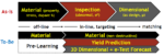
The front-end design team needs to know the power, performance and area of a given design iteration. This information drives optimization, and before iSpatial, the front-end team needed to wait for a completed design iteration from the back-end team to know these results. That could take many days.

Instead, with the iSpatial flow, the front-end design team gets meaningful and actionable information very quickly on things like overall performance, size and power as well as details on items such as routing congestion, critical path delays and clock insertion delays. The information is also presented in a format that is familiar to the front-end design team, avoiding the need to get an interpretation of the data from the back-end team. This contributes to efficiency as well as quality of results.

So, the integrated iSpatial flow minimizes turnaround time and maximizes efficiency for design iterations. But there’s more—the flow can reduce the overall number of design iterations as well. This is one application of ML. In this case, the tool will “learn” from prior design iterations and apply that knowledge in the form of suggestions for the next design iteration. Vivek provided some examples, things like modified pin placement to avoid DRC errors or a different choice of cell library elements that will improve performance. These suggestions are provided in the form of scripts that can be run to implement the various suggestions. This technology can actually help reduce design iterations by avoiding errors, which is headline news from a schedule perspective. Cadence calls these learning and optimization techniques “ML outside”.

There’s another ML use model which applies the technology to the core algorithms to optimize the results achieved. Cadence calls this “ML inside”. I explored some examples of these techniques with Vivek as well. Delay calculation was one we discussed. This is a very iterative and time-consuming process, requiring simulation. ML can optimize this process to increase both the speed of results as well as accuracy. Synthesis mapping is another example, where the best choice for a given implementation can be “learned” to avoid additional iterations.

Kam provided some more color on “ML inside” techniques at Cadence. Consider that many EDA algorithms are iterative in nature and the starting point for those iterations can impact the time to a converged result, or even if there is convergence at all. Finding the right starting point is something of a pattern-matching problem, and ML is quite good at those kinds of tasks.

As a final point, I asked about actual results on real customer designs. Kam reminded me that some detailed statistics were shared in the original press release, an unusual level of detail for a press release actually. MediaTek reported, “… we were able to automatically and quickly train a model of our CPU core, which resulted in an improved maximum frequency along with an 80% reduction in total negative slack. This enabled 2X shorter turnaround time for final signoff design closure.”

Samsung Electronics reported, “(iSpatial) enabled us to achieve 3X faster design turnaround time by quickly iterating on RTL, constraints and floorplan while improving total power by 6%. Furthermore, Cadence’s unique ML capabilities allowed us to train a model of our design on Samsung Foundry’s 4nm EUV node, which helped us further achieve a 5% performance improvement and 5% leakage power savings.”

Kam further mentioned that on several advanced customer designs, a double-digit total negative slack (TNS) improvement, often 50 percent or more, was achieved. On these same designs, power was improved by 1 to 3.5 percent. If you consider that a design team could spend months looking for a three percent power improvement, these numbers are quite impressive. Kam also explained that design groups using older technology nodes are also seeing benefits from the new flow in terms of reduced design iterations and a more finely tuned methodology.

At this point, I felt like I had seen the future (of chip design). You can learn more about the Cadence suite of digital design and signoff products here.


A Compelling Application for AI in Semiconductor Manufacturing

A Compelling Application for AI in Semiconductor Manufacturing
by Tom Dillinger on 07-06-2020 at 6:00 am

AI opportunities

There have been a multitude of announcements recently relative to the incorporation of machine learning (ML) methods into EDA tool algorithms, mostly in the physical implementation flows.  For example, deterministic ML-based decision algorithms applied to cell placement and signal interconnect routing promise to expedite and optimize physical design results, without the iterative cell-swap placement and rip-up-and-reroute algorithms.  These quality-of-results and runtime improvements are noteworthy, to be sure.

Yet, there is one facet of the semiconductor industry that is (or soon will be) critically-dependent upon AI support – the metrology of semiconductor process characterization, both during initial process development/bring-up, and in-line inspection driving continuous process improvement.  (Webster’s defines metrology as “the application of measuring instruments and testing procedures to provide accurate and reliable measurements”.)  Every aspect of semiconductor processing, from lithographic design rule specifications to ongoing yield analysis, is fundamentally dependent upon accurate and reliable data for critical dimension (CD) lithographic patterning and material composition.

At the recent VLSI 2020 Symposium, Yi-hung Lin, Manager of the Advanced Metrology Engineering Group at TSMC, gave a compelling presentation on the current status of semiconductor metrology techniques, and the opportunities for AI methods to provide the necessary breakthroughs to support future process node development.  This article briefly summarizes the highlights of his talk. [1]

The figure below introduced Yi-hung’s talk, illustrating the sequence where metrology techniques are used.  There is an initial analysis of fabrication materials specifications and lithography targets during development.  Once the process transitions to manufacturing, in-line (non-destructive) inspection is implemented to ensure that variations are within the process window for high yield.  Over time, the breadth of different designs, and specifically, the introduction of the process on multiple fab lines requires focus on dimensional matching, wafer-to-wafer, lot-to-lot, and fab line-to-fab line.

The “pre-learning” opportunities suggest that initial process bring-up metrology data could be used as the training set for AI model development, subsequently applied in production.  Ideally, the models would be used to accelerate the time to reach high-volume manufacturing.  These AI opportunities are described in more detail below.

Optical Critical Dimension (OCD) Spectroscopy
I know some members of the SemiWiki audience fondly (or, perhaps not so fondly) recall the many hours spent in the clean room looking through a Zeiss microscope at wafers, to evaluate developed photoresist layers, layer-to-layer alignment verniers, and material etch results.  At the wavelength of the microscope light source, these multiple-micrometer features were visually distinguishable – those days are long, long gone.

Yi-hung highlighted that OCD spectroscopy is still a key source of process metrology data.  It is fast, inexpensive, and non-destructive – yet, the utilization of OCD has changed in deep sub-micron nodes.  The figure below illustrates the application of optical light sources in surface metrology.

The incident (visible, or increasingly, X-ray) wavelength is provided to a 3D simulation model of the surface, which solves electromagnetic equations to predict the scattering.  These predicted results are compared to the measured spectrum, and the model is adjusted – a metrology “solution” is achieved when the measured and EM simulation results converge.

OCD illumination is most applicable when an appropriate (1D or 2D) “optical grating-like” pattern is used for reflective diffraction of the incident light.  However, the challenge is that current surface topographies are definitely three-dimensional, and the material measures of interest do not resemble a planar grating.  Optical X-ray scatterometry provides improved analysis accuracy with these 3D topographies, but is an extremely slow method of data gathering.

Yi-hung used the term ML-OCD, to describe how an AI model derived from other metrology techniques could provide an effective alternative to the converged EM simulation approach.  As illustrated below, the ML-OCD spectral data would serve as the input training dataset for model development, with the output target being the measures from (destructive) transmission electron microscopy (TEM), to be discussed next.

ML for Transmission Electron Microscopy (TEM)
TEM utilizes a focused electron beam that is directed through a very thin sample – e.g., 100nm or thinner.  The resulting (black-and-white) image provides high-magnification detail of the material cross-section, due to the much smaller electron wavelength (1000X smaller than an optical photon).

There are two areas that Yu-hing highlighted where ML techniques would be ideal for TEM images.  The first would utilize familiar image processing and classification techniques to automatically extract CD features, especially useful for “blurred” TEM images.  The second would be to serve as the training set output for ML-OCD, as mentioned above.  Yi-hung noted that one issue to the use of TEM data for ML-OCD modeling is that a large amount of TEM sample data would required as the model output target.  (The fine resolution of the TEM image compared to the field of the incident OCD exposure exacerbates the issue.)

ML for Scanning Electron Microscopy (SEM)
The familiar SEM images measure the intensity of secondary electrons (emitted from the outer atomic electron shell) that are produced from collisions with an incident primary electron – the greater the number of SE’s generated in a local area, the brighter the SEM image.  SEMs are utilized at deep submicron nodes for (top view) line/space images, and in particular, showing areas where lithographic and material pattering process defects are present.

ML methods could be applied to SEM images for defect identification and classification, and to assist with root cause determination by correlating the defects to specific process steps.

Another scanning electron technique uses a variable range of higher-energy primary electrons, which will have different landing distances from the surface, and thus, provide secondary electrons from deeper into the material.  However, an extremely large primary energy will result in the generation of both secondary electrons and X-ray photons, as illustrated below.  (Yi-hung noted that this will limit the image usability for the electron detectors used in SEM equipment, and thus limit the material depth that could be explored – either more SE sensitivity or SE plus X-ray detector resolution will be required.)   The opportunities for a (generative) machine learning network to assist with “deep SEM” image classification are great.

Summary
Yi-hung concluded his presentation with the following breakdown of metrology requirements:

  • (high-throughput) dimensional measurement:
      • OCD, X-ray spectroscopy  (poor on 3D topography)
  • (high-accuracy, destructive) reference measurement:  TEM
  • Inspection (defect identification and yield prediction):  SEM
  • In-line monitoring (high-throughput, non-destructive):
      • hybrid of OCD + X-ray, with ML-OCD in the future?

In all these cases, there are great opportunities to apply machine learning methods to the fundamental metrology requirements of advanced process development and high-volume manufacturing.   Yi-hung repeated the cautionary tone that semiconductor engineering metrology currently does not have the volume of training data associated with other ML applications.  Nevertheless, he encouraged data science engineers potentially interested in these applications to contact him.   🙂

Yu-hing also added that there is a whole other metrology field to explore for potential AI applications – namely, application of the sensor data captured by individual pieces of semiconductor processing equipment, as it relates to overall manufacturing yield and throughput.  A mighty challenge, indeed.

-chipguy


References

[1]  Yi-hung Lin, “Metrology with Angstrom Accuracy Required by Logic IC Manufacturing – Challenges From R&D to High Volume Manufacturing and Solutions in the AI Era”, VLSI 2020 Symposium, Workshop WS2.3.

Images supplied by the VLSI Symposium on Technology & Circuits 2020.


Teaching AI to be Evil with Unethical Data

Teaching AI to be Evil with Unethical Data
by Matthew Rosenquist on 07-05-2020 at 2:00 pm

Teaching AI to be Evil with Unethical Data

An Artificial Intelligence (AI) system is only as good as its training. For AI Machine Learning (ML) and Deep Learning (DL) frameworks, the training data sets are a crucial element that defines how the system will operate. Feed it skewed or biased information and it will create a flawed inference engine.

MIT recently removed a dataset that has been popular with AI developers. The training set, 80 Million Tiny Images, was scraped from Google in 2008 and used in training AI software to identify objects. It consists of images that are labeled with descriptions. During the learning phase, an AI system will ingest the dataset and ‘learn’ how to classify images. The problem is that many of the images are questionable and the labels were inappropriate. For example, women are described with derogatory terms, body parts are identified with offensive slang, and racial slurs were sometimes used to label minority people. Such training should never be allowed.

AI developers need vast amounts of training data to train their systems. Collections are often created out of convenience, without consideration for courteous content, copyright restrictions, compliance to licensing agreements, people’s privacy rights, or respect for society. Unfortunately, many of the available sets were haphazardly created by scraping the internet, social sites, copyrighted content, and human interactions without approval or notice.

Many of the most used training datasets have issues. A large number were created by unethically acquiring content, some contain derogatory or inflammatory information, and for others, the sample is not representative because it excludes certain groups that would benefit from inclusion.

The problem has become worse over time. Flawed datasets, that were made openly available to the developer community early-on, became so popular that they are now considered a standard. These benchmarks are used to check accuracy and performance across different AI systems and configurations.

Too few are vetted for inclusion, content, accuracy, or socially acceptable content. Using such flawed records is simply unethical because the resulting systems can be racially charged, biased, and promote inequality.

We cannot have good AI if the commonly used datasets create unethical systems. All files should be vetted and both the creators and product developers held responsible. Just as chefs are held accountable for the ingredients they put into their prepared dishes, so should the AI community be held responsible for allowing poor data to result in harmful AI systems.


Application-Specific Lithography: The 5nm 6-Track Cell

Application-Specific Lithography: The 5nm 6-Track Cell
by Fred Chen on 07-05-2020 at 10:00 am

Application Specific Lithography The 5nm 6 Track Cell

An update is now available here: Application-Specific Lithography: Patterning 5nm 5.5-Track Metal by DUV

The 5nm foundry (e.g., TSMC) node may see the introduction of 6-track cells (two double-width rails plus four minimum-width dense lines) with a minimum metal pitch in the neighborhood of 30 nm. IMEC had studied a representative case as its ‘7nm’ case [1]. TSMC had some published 5nm test structures which looked like extended 6-track cells [2]. Even with EUV lithography, the use of highly specialized patterning techniques is expected. We consider various options here for patterning the lines of the 6-track cell (Figure 1).

Figure 1. Reference example for 5nm 6-track cell with four 14 nm metal lines spaced 14 nm apart, and two 28 nm wide rails at the upper and lower boundaries.

Single Exposure EUV

At first glance, a single exposure technique using EUV should be easiest to carry out without much yield consideration. However, EUV has many added concerns uncovered over the years such as stochastic variation [3-5]. Figure 2 shows the map of pupil sources correlated with the possible diffraction patterns for a 154 nm pitch 6-T cell (14 nm internal half-pitch, 28 nm rail width). Unfortunately, each individual diffraction pattern takes less than 20% pupil fill, leading to throughput loss for a dedicated diffraction pattern on the current NXE:3400B systems [6].

Figure 2. All possible diffraction patterns for a single EUV 0.33 NA exposure of the 6-track cell line pattern in Figure 1. Each different symbol represents a diffraction pattern produced by the corresponding EUV source point, labeled by a 7-digit string. The nth digit indicates how many -nth, nth orders are included (0, 1 or 2).

When the illumination is expected to spread the photon number over at least several diffraction patterns, each source point effectively becomes more noisy [5].

SAQP

A more familiar alternative, but not without its own technical challenges, is self-aligned quadruple patterning (SAQP), using immersion lithography. Conducting features are best defined between spacers to make cutting more efficient; this is also known as the “spacer-is-dielectric” (SID) approach [7]. The biggest hurdle is that the number of spacers is naturally even, so that the features defined between spacers will naturally come in odd numbers. As a workaround, some spacers may be made to disappear or merge, with a deliberately narrowed space between some starting features. Effectively, this removes one spacer to leave an odd number of spacers, with an even number of features in between. For the 154 nm pitch case being studied, the starting pattern proposed in [1] could actually be drawn as a 308 nm pitch pattern as shown in Figure 3.

Figure 3. SAQP integration for 6-track cell. Blue: starting (core or mandrel) features. Green: 1st spacer. Red: 2nd spacer. Purple: dielectric masked by 2nd spacer. Gray: metal filling in between spacers. In some schemes, the material filled at the 1st spacer locations is different from that filled at other locations between the 2nd spacers. This is to facilitate self-aligned blocking [1].

Pitch Walking

Due to the breaking of symmetry in the pattern of Figure 1, “pitch walking” is likely to occur in the patterning process. This is the effect where the spacing between some lines is decreased or increased relative to the spacing between other lines. This can occur in the lithography process itself, due to defocus, for either the EUV or SAQP options described above.

For the EUV case, the different illumination source points can produce different effects (Figure 4). This is again aggravated by stochastic sensitivity.

Figure 4. Defocus can cause pitch walking to an extent dependent on the source points for illumination. The conditions assumed for this 6-track cell example are 154 nm pitch, 13.5 nm wavelength, 0.33 NA, 50 nm defocus.

For the SAQP case, there are additional potential contributors to pitch walking from process steps following the lithography, such as spacer deposition thickness and spacer overetch. These extra conditions force tighter tolerances on defocus for the starting features, so that even 30 nm could be limiting (Figure 5).

Figure 5. For SAQP, defocus tolerance needs to be tighter to prevent pitch walking caused by post-litho process steps.

A potential mitigation of the defocus impact is to use a multi-patterning technique instead of a symmetry-breaking single exposure for the SAQP starting features. In the most brute-force case, 3 exposures, 3 etches may be used to each pattern one of the three starting features (the central 56 nm and the two side 42 nm features) within the 308 nm pitch. A more efficient way would be to use self-aligned triple patterning (SATP) [8] to define all three features with one mask (Figure 6). For this process, the lithography will maintain repeating feature symmetry.

Figure 6. SATP flow [8] using two spacers for producing the starting features for SAQP shown in Figure 3.

Other steps that can be taken to address pitch walking for SAQP include thickness optimization [9] and process control loop feedback [10]. Presumably, the same issues have been encountered for self-aligned double patterning (SADP) already, so as SADP matures, SAQP should benefit.

Self-aligned blocking or cutting

The breaks in the line tracks also need to be patterned. Within the same EUV exposure as the lines, the extra pitches in the second dimension create more diffraction patterns among which the EUV photon number will be divided [5], further aggravating the stochastic effects. Line ends are already small collection areas for photons [11], leading to extra tip-to-tip variation. The classical resolution limit for line end gaps is ~ 0.6 wavelength/NA [12], where NA is the numerical aperture of the lithography system (~25 nm for the NXE:3400 with 0.33 NA). Thus, a separate exposure for cutting the lines, or blocking the etch at some locations, is preferred.

The self-aligned block (SAB) approach is preferred over a single exposure block or cut, due to its being more robust against overlay and edge placement errors [1,13]. However, the SAB approach necessitates the use of two masks, as two oppositely selective etches will be used for different block/cut locations. While EUV is commonly discussed for use in the SAB approach, immersion lithography can also be used, with self-aligned double patterning (SADP) as needed [14].

Summary of approaches

The pros and cons of the approaches covered above are summarized in the table below:

References

[1] J. U. Lee, S. H. Choi, Y. Sherazzi, R. R. H. Kim, “SAQP spacer merge and EUV self-aligned block decomposition at 28nm metal pitch on imec 7nm node,” Proc. SPIE 10962, 109620N (2019).

[2] G. Yeap, S. S. Lin, Y. M. Chen, H. L. Shang, P. W. Wang, H. C. Lin, Y. C. Peng, J. Y. Sheu, M. Wang, X. Chen, B. R. Yang, C. P. Lin, F. C. Yang, Y. K. Leung, D. W. Lin, C. P. Chen, K. F. Yu, D. H. Chen, C. Y. Chang, H. K. Chen, P. Hung, C. S. Hou, Y. K. Cheng, J. Chang, L. Yuan, C. K. Lin, C. C. Chen, Y. C. Yeo, M. H. Tsai, H. T. Lin, C. O. Chui, K. B. Huang, W. Chang, H. J. Lin, K. W. Chen, R. Chen, S. H. Sun, Q. Fu, H. T. Yang, H. T. Chiang, C. C. Yeh, T. L. Lee, C. H. Wang, S. L. Shue, C. W. Wu, R. Lu, W. R. Lin, J. Wu, F. Lai, Y. H. Wu, B. Z. Tien, Y. C. Huang, L. C. Lu, J. He, Y. Ku, J. Lin, M. Cao, T. S. Chang, S. M. Jang, “5nm CMOS Production Technology Platform featuring full-fledged EUV, and High-Mobility Channel FinFETs with densest 0.021 um2 SRAM cells for Mobile SOC and High Performance Computing Applications,” IEDM 2019.

[3] A. Frommhold, D. Cerbu, J. Bekaert, L. Van Look, M. Maslow, G. Rispens, E. Hendrickx, “Predicting Stochastic Defects across the Process Window,” Proc. SPIE 11147, 1114708 (2019).

[4] P. De Bisschop, E. Hendrickx, “Stochastic Printing Failures in EUV Lithography,” Proc. SPIE 10957, 109570E (2019).

[5] https://www.linkedin.com/pulse/stochastic-variation-euv-source-illumination-frederick-chen/

[6] M. van de Kerkhof, H. Jasper, L. Levasier, R. Peeters, R. van Es, J-W. Bosker, A. Zdravkov, E. Lenderink, F. Evangelista, P. Broman, B. Bilski, T. Last, “Enabling sub-10nm node lithography: presenting the NXE:3400B EUV scanner,” Proc. SPIE 10143, 101430D (2017).

[7] Y. Ban, D. Z. Pan, “Self-aligned double-patterning layout decomposition for two-dimensional random metals for sub-10-nm node design,” J. Micro/Nanolith. MEMS MOEMS 14, 011004 (2014).

[8] J-Y. Lee, J-S. Park, S-G. Woo, US Patent 7842601, assigned to Samsung, filed Apr. 20, 2006.

[9] T. Yang, D. Yim, “SAQP Pitch walking improvement pathfinding by simulation,” 41st International Symposium on Dry Process, 2019. http://www.dry-process.org/2019/poster_program.html

[10] H. Ren, A. Mani, S. Han, X. Li, X. Chen, D. Van Den 90Heuvel, “Advanced process control loop for SAQP pitch walk with combined lithography, deposition and etch actuators,” Proc. SPIE 11325, 1132523 (2020).

[11] https://www.linkedin.com/pulse/photon-shot-noise-impact-line-end-placement-frederick-chen/

[12] https://www.linkedin.com/pulse/lithography-resolution-limits-line-end-gaps-frederick-chen

[13] A. Raley, N. Mohanty, X. Sun, R. A. Farrell, J. T. Smith, A. Ko, A. W. Metz, P. Biolsi, A. Devilliers, “Self-Aligned Blocking Integration Demonstration for Critical sub 40nm pitch Mx Level Patterning,” Proc. SPIE 10149, 101490O (2017).

[14] E.g., see A. J. deVilliers, US Patent 9240329, assigned to Tokyo Electron Limited, filed Feb. 17, 2015.

The original article first appeared in LinkedIn Pulse: Application-Specific Lithography: The 5nm 6-Track Cell

Related Lithography Posts


What is Zero Trust Model (ZTM)

What is Zero Trust Model (ZTM)
by Ahmed Banafa on 07-05-2020 at 10:00 am

What is Zero Trust Model ZTM

The Zero Trust Model of information #security simplifies how #information security is conceptualized by assuming there are no longer “trusted” interfaces, applications, traffic, networks, or users. It takes the old model— “trust but verify”—and inverts it, because recent breaches have proven that when an organization trusts, it doesn’t verify [6].

This model requires that the following rules be followed [6]:

  • All resources must be accessed in a secure manner.
  • Access control must be on a need-to-know basis and strictly enforced.
  • Systems must verify and never trust.
  • All traffic must be inspected, logged, and reviewed.
  • Systems must be designed from the inside out instead of the outside in.

The zero-trust model has three key concepts:

  • Ensure all resources are accessed securely regardless of location.
  • Adopt a least privilege strategy and strictly enforce access control.
  • Inspect and log all traffic.

“Outside-In” to “Inside-Out” Attacks
According to a Forrester Research report, information security professionals should readjust some widely held views on how to combat cyber risks. Security professionals emphasize strengthening the network perimeter, the report states, but evolving threats—such as increasing misuse of employee passwords and targeted attacks—mean executives need to start buffering internal networks. In the zero-trust security model, companies should also analyze employee access and internal network traffic. One major recommendation of the Forrester report is for companies to grant minimal employee access privileges. It also emphasizes the importance of log analysis; another recommendation is for increased use of tools that inspect the actual content, or data “packets,” of internal traffic [1].

Teams within enterprises, with and without the support of information technology management, are embracing new technologies in the constant quest to improve business and personal effectiveness and efficiency. These technologies include virtualization; cloud computing; converged data, voice, and video networks; Web 2.0 applications; social networking; #smartphones; and tablets. In addition, the percentage of remote and mobile workers in organizations continues to increase and reduce the value of physical perimeter controls [2].

The primary vector of attackers has shifted from “outside-in” to “inside-out.” Formerly, the primary attack vector was to directly penetrate the enterprise at the network level through open ports and to exploit operating system vulnerabilities. We call this attack methodology “outside-in.” In “inside-out” attacks, the user inside the “protected” network reaching out to an external website can be just as vulnerable as the user accessing the Internet from home [5].

Zero Trust Recommendations:

  • Update network security with next-generation firewalls.
  • Use a “sandbox” control to detect unknown threats in files.
  • Establish protected enclaves to control user access to applications and resources.
  • Use a specialized anti-phishing email protection service.
  • Use threat intelligence to prioritize vulnerability remediation.
  • Analyze logs using advanced machine learning algorithms to detect compromised and malicious users.
  • Implement an incident management system to minimize the impact of individual incidents.
  • Deploy a cloud services manager to discover, analyze, and control shadow IT. (Shadow IT is hardware or software within an enterprise that is not supported by the organization’s central IT department.)
  • Monitor your partners’ security postures using a cloud-based service.
  • Deploy an enterprise key & certificate management system.
  • Deploy a backup, cloud-based DDoS mitigation service.
  • Deploy a non-signature-based endpoint malware detection control.

Just remember: the zero-trust model of information security means “verify and never trust.”

Ahmed Banafa, Author the Books:
Secure and Smart Internet of Things (IoT) Using Blockchain and AI

Blockchain Technology and Applications

Read more articles at: https://medium.com/@banafa

References:

[1] http://www.securitymanagement.com/article/zero-trust-model-007894

[2] http://www.securityweek.com/steps-implementing-zero-trust-network

[3] http://spyders.ca/reduce-risk-by-adopting-a-zero-trust-modelapproach-to-security/

[4] http://www.cymbel.com/zero-trust-recommendations/

[5] http://csrc.nist.gov/cyberframework/rfi_comments/040813_forrester_research.pdf

[6] https://go.forrester.com/research/


The Time Has Arrived for AI Based Data Twinning! Shrink the Pipe while Increasing Data Fidelity

The Time Has Arrived for AI Based Data Twinning! Shrink the Pipe while Increasing Data Fidelity
by Tom Freeman on 07-05-2020 at 6:00 am

AI Based Data Twinning

Time to Change our Thinking:
It is time to work the other side of the communications equation. Send less data. But apply new synthetic data science and machine learning to get more and richer information: a way that requires the transfer of radically fewer actual bits – perhaps 1 or 2% of the bits – but with higher model fidelity. The time for AI based Data Twinning has arrived.

The Conundrum:
If you make cars smart enough to support comms-free autonomy then you’ve more than doubled, and perhaps tripled, the price of basic transportation. If you rely on comms for off-board intelligence then autonomous mobility is geo-fenced to areas that have brilliant LTE Broadband and 5G without “LTE-Brownouts,” “Not-Spots,” or “LTE deserts”.

The graph above demonstrates how the LTE broadband through-put behaves at a stationary position during the course of a day. Low Earth Orbit (LEO) mobile satellite broadband solution-set overlay for OEM vehicles is having challenges getting to market. Not a happy situation.

The Data Requirement:
The data communications requirement, as estimated by the Automotive Edge Computing Consortium[1], for a fleet of 100 million autonomous vehicles will be measured in the thousands of exabytes per month with latencies measured variously, by applications, in weeks, minutes, and seconds. The data demand of millions of additional AVs per year will swamp any communication system. Even if you gave away the autonomous vehicle application and all the associated hardware, the data cost would make autonomy affordable only for the wealthy.

The Big Idea: Shrink the pipe but increase fidelity
It is time to work the other side of the equation. Send less data. Get more and richer information, but do so in a way that requires the transfer of radically fewer actual bits – perhaps 1 or 2% of the bits. This approach opens up non-broadband communications technologies that are designed to cover wider areas and long distances like NB IoT and LTE-M. These systems are less design intrusive on the vehicle than today’s Ku space antennas, and the terrestrial towers are already in place. For those hard to reach places, LEO L band antennas are already integrated with shark fins. Profoundly fewer bits transmitted means profoundly smaller data bills delivering happier OEMs and consumers.

Data Twinning: shrink the pipe, increase the fidelity
The solution to this conundrum is to obviate the requirement for Always-On full broadband and full data transfer of data between the vehicle and the cloud and back to vehicle. The requirement is to set the data transfer at the lowest possible level and then work on getting the highest quality, physically accurate simulation data mirrored in cloud and car. Send enough data to confirm the expected and send complex data for the unexpected. The rest of the reality would be synthetically recreated using visual, non-visual, LiDAR, RADAR modeling on both ends. As more data is twinned, the smaller the pipe needs be. Eventually it is very small.


The graph above illustrates the more data that is twinned the smaller the pipe to keep it fresh needs be.

Data Twinning requires more than visual images
Companies like Rendered.ai have combined physics based synthetic data and AI. This means that the objects that the AI is trained on are not based on an AI game-engine model of the world, instead they are trained on physics based synthetic data. What is important here is that these physic-based objects have accurate light transfer characteristics and fully ray traced caustics which improves realism that delivers ground truth. The result is that synthetic data can be used for machine learning, testing data sets, and twinning.


This approach allows for physically accurate simulations of non-visual data (LiDAR, RADAR – including active scanning and SAR/IR and Ultrasound.) Full-wave electromagnetic simulations of RADAR and other common and novel sensors allow for a richer picture of the ground truth than visual images alone. Vehicles are sensor-rich environments and data from other vehicle sensors can be repurposed for the twinning applications.

The Point:
Synthetic, visual, non-visual plus vehicle data can simultaneously accurately recreate the ground truth in the cloud and the network truth in the vehicle to provide for safe autonomy in high and low connectivity environments.

So, who is pioneering this radical approach to data transfer?
Companies like Rendered.ai (www.rendered.ai) work in concert with existing AI simulation tools and data repositories for adding novel data types. These additions accelerate AI efforts by improving data labeling, and fortify AI against edge conditions, concept drift and model decay. This package integrates new data-types from the vehicle and highway-based sensors and measure their efficacy. Additionally, using a Data Science friendly cloud native workflow, Rendered.ai integrates visual and non-visual data and improves the control of simulations by the data scientist for safer autonomy and more robust data insights.

Image courtesy of Rendered.ai

[1] AECC January 2020 Whitepaper: General Principal and Vision https://aecc.org/

Tom Freeman
I have worked for the best part of the last 10 years on the problem of satellite broadband to the vehicle and all the associated challenges. Changes in the ground and space segment landscape in the last quarter played into my growing anxiety that even if we committed every bit of deployed, planned and dreamt of LEO capacity to vehicle communication it would not be enough. Enough for infotainment perhaps, but not for the core consumption of AVs cloud to vehicle to cloud throughput for network, cruise assist, HD mapping and all the others.


Tears in the Rain – Arm and China JVs

Tears in the Rain – Arm and China JVs
by Jay Goldberg on 07-03-2020 at 10:00 am

Tears in the Rain – Arm and China JVs

We always warn clients that even in the best of times, Joint Ventures (JVs) in China always end in tears. And we are far from the best of times right now. There is a major example of this playing out right now with Arm China.

Arm’s China JV is, to put it simply, a bit of a mess. The Board has fired the CEO, but he has refused to leave. And owing to some peculiarities of Chinese corporate law, removing him is proving difficult.

We wanted to take a look at that as an example of the many complexities of doing business in China. We want to be clear this is not intended as a criticism of Arm. Their plight today is very much a function of the overall business climate, and there are many forces at play beyond their control.

Some quick background. Arm makes what are essentially blueprints for processors, a crucial part of many chips. Think of Arm cores as the engine of a car. Arm provides the latest designs for the engine, then the car makers put all the other pieces on top. Processors, the engine in this analogy, are expensive to design but relatively common across many part of the function sof a chip. So almost every chip which does any form of computation (as opposed to just basic sensing and reacting) uses Arm intellectual property (IP).

This role puts Arm in a central position for any semis strategy, and so it should come as no surprise that Arm started to draw a lot of scrutiny in China. As many foreign companies discovered in the early part of the 2010’s, the Chinese government was very interested in chips and looking to build its own, domestic chip companies. This led to pressure being applied to many foreign chip providers. Then the US-China Trade War hit, further ratcheting up the pressure. In the end, the Arm parent sold a 51% stake in Arm China to a consortium of Chinese investors.

Background on the deal is a bit fuzzy. There is no Arm press release on the deal, only a brief release from parent Softbank. They describe the rationale for the deal in pretty basic terms:

The Chinese market is valuable and distinctive from the rest of the world. Arm believes this joint venture, which will license Arm semiconductor technology to Chinese companies and locally develop Arm technology in China, will expand Arm’s opportunities in the Chinese market.

Source: SoftBank

This piece from Reuters says Arm sold 51% to a consortium of Chinese investors including private equity vehicle Hou An.

Backers of Hou An include sovereign wealth fund China Investment Corporation, Silk Road Fund, Singapore’s Temasek Holdings [TEM.UL], Shenzhen’s Shum Yip Group and Hopu, according to China’s Ministry of Science and Technology.

Source: Reuters

Crucially, the article points out that:
Arm will, however, continue to get a significant proportion of all license, royalty, software and services revenue earned by Arm China’s licensing of its chips, SoftBank said.

Source: Reuters

So right from the get-go. There is something odd going on here. First, Softbank’s rationale states that the China market is “distinctive”. By which they presumably mean it is distinctive in that the government has a strong, but unofficial policy to “encourage” foreign IP transfers.

Second, Arm is giving up 51% control but still hopes to get a significant portion of the JV’s revenue. One would think that for the $775 million it received and the loss of voting control would mean it no longer has a claim on the JV ‘s revenues.

We have an interpretation of all this based on our many years of working with China JVs. So allow a simple, if imprecise, description. China wants Arm to transfer IP to China, and probably cut better royalty rates for Chinese chip companies. Arm sees it has no choice, and wants to keep its China business on a sound footing. So they set up the JV. They give up 51% control, which theoretically qualifies the JV as a Chinese company, thus satisfying the government. The JV has the right to sell Arm IP in China, and a portion of that is passed on to the parent as a supplier of IP.

But here is the tricky bit. Arm no longer has voting control of the company, they are less than 50%. How do they maintain effective control over a sizable and strategically important part of their business? One method we have seen other companies use is to diversify the holders of that 51%. This way the foreign company may not have majority control, but it does have a plurality as the largest single shareholder.

Then the problem becomes how to manage the various other shareholders and ensure that when push comes to shove, the foreign company still can muster up at least a few more points in any vote. Most US companies we have seen do this by relying on the fact that China is not a monolith. The various JV partners will all act in their own interests. For the most part, that means they will vote their JV shares to whatever will maximize the value of the JV. When issues of national policy arise, they may unify to vote against the foreigner, but most of the other times, they will likely have divergent viewpoints, which the 49% foreign-holder can manage to reach any desired outcome. This is always complicated, and a big part of the reason JVs fail (in most places, not just China).

Over the years, we have worked with dozens of China JVs, probably over 100. They almost always run into problems. We know dozens of examples where one party will walk out the door with customer lists, product designs, the entire management team – pretty much anything of value. To be fair, we have also seen countless examples of Western companies being equally ruthless leaving their JV partner with nothing.

In Arm’s case, something has clearly gone wrong. The Financial Times has been doing the best reporting on this (and here) . Simplifying again, the CEO of Arm China was accused of conflicts of interest. He has set up an investment fund, and is accused of offering discounts on Arm licenses to companies who invest in his fund. Sounds bad, but this is very far from the worst JV horror story we have seen.

So after some period of negotiation, the board of Arm China voted to remove him. However, he holds all the official documents and stamps for the JV, and he has refused to step down. He appeared as the CEO of Arm China in a keynote at an industry event last week. Chinese company law makes removing him at this stage possible, but complicated and time-consuming. The assumption is that he is making things difficult to bolster his position in an ultimate exit negotiation. For the moment he has a lot of leverage by having possession of the seals, but also through the presumed loyalty of much of the local team.

So far it is unpleasant but fairly straightforward. However, the FT story that came out this weekend adds a few wrinkles that make the story positively weird.

Going back to the way that foreign companies can maintain control with less than 50% control of a JV. Foreign companies often find they are dealing with a sea of strangers. All those private equity funds are helpful, but how to gauge where their true interests lay. Wouldn’t it be helpful to have some known actor have a stake in the JV, to provide those extra votes? How about someone who has been an employee for almost 20 years and now runs the China business? Maybe let him invest in the JV, “aligning” his incentives in lieu of some form of restricted stock. It turns out that among the investing consortium who acquired 51% of Arm China, the CEO ended up with 13% of the JV.

It really looks like Arm thought they had found an elegant solution to the trust issues embedded in every JV, but instead have created a bigger problem.

Further complicating the matter is that it appears that at least some of the Arm China board members not only knew about the CEO’s fund, but invested in it themselves. It seems possible that Arm signed off on the fund without perhaps understanding all the details. Part of Arm’s work everywhere is incubating new chip companies which can grow to be big Arm customers. Nowhere is this more important than in China which has 1,000+ new chip companies. So Arm China is working with numerous chip incubators, including the CEO’s firm.

Further complicating the matter is that the principals in this affair are a who’s who of executives from China’s leading chip companies.

Our favorite detail to emerge from this is that the Arm China CEO named one of his holding shell companies “Acorn Spring Limited”. The original name of Arm Holdings is Acorn RISC Machines”, so there is an interesting bit of irony in that.

And then there is the matter of Huawei

When Arm sold its stake in Arm China, one assumption in the US was that part of the motivation was to allow Arm, a British firm owned by a Japanese conglomerate, to continue licensing IP to Huawei. Like every other chip designer, Huawei relies heavily on Arm. And there are concerns that the US government will prevent Arm from supplying Huawei. In the first round of Huawei restrictions last year, Arm made it known that they were only providing Huawei IP from current licenses and were cutting off access to future improvements. With Arm’s complex China holding structure, we can think of a half dozen loopholes that may allow Huawei to continue to access Arm IP. Maybe they take advantage of those, maybe not.

And this gets us back to the root of the problem. The entire notion of Joint Ventures has always been a regulatory hack. China has wanted to limit foreign companies’ control of China’s market. Through various iterations, the JV has been a way for Chinese companies to benefit from foreign companies operating in China, from profit sharing to IP transfer. For almost a decade now, JVs have been on the wane as China’s corporate laws have matured, diminishing the value of the structure. But they persist, especially in sectors the government views as crucial.

JVs introduce so many problems. At heart, they are management by committee. The parties in the JV have conflicting interests, and these conflicts are the reason we almost never see JVs outside of China. There is always a rivalry for control and sharing of gains. These usually lead to internal rifts inside a company, forcing managers and employees to choose sides. Arm is not alone in their struggle, they are just the latest, most public example of the problems that arise with these structures.

We are not sure how this will end. If we had to guess, we think it is likely that the CEO leaves in the coming months. He will likely go with a nice severance package and Arm China will continue to work with his incubator fund. It is quite the soap opera.

Reference: DIGITS TO DOLLARS


Fast and Accurate Variation-Aware Mixed-Signal Verification of Time-Domain 2-Step ADC

Fast and Accurate Variation-Aware Mixed-Signal Verification of Time-Domain 2-Step ADC
by Daniel Nenni on 07-03-2020 at 6:00 am

Solido SemiWiki

My favorite old school Solido Graphic!

There is an interesting white paper out from Mentor on how a customer used the Solido Varation Designer tool to reduce Monte Carlo simulations. As you may know I worked for Solido for 10+ years up until they were acquired by Mentor in December of 2017. It was an incredible personal and professional experience. I have the highest respect for the Solido Saskatoon development team which is why I wanted to do this white paper Q&A with Nebabie Kebebew, Sr. Product Manager, AMS Verification, Mentor, a Siemens Business.

Fast and Accurate Variation-Aware Mixed-Signal Verification of Time-Domain 2-Step ADC “To meet today’s analog-to-digital converter (ADC) specifications and to produce a high-yield design, teams typically need to perform extensive brute force mixed-signal simulations to account for all potential design variation. However, at nanometer nodes, the number of process, voltage and temperature (PVT) corners and parametric variation grow exponentially making the simulation impractical and costly. Teams attempt to employ extrapolation methods to shorten verification times. Learn how Analog Value Ltd. instead used Solido™ Variation Designer™ to perform PVT corner and Monte Carlo Simulation all at once to reduce simulations by orders of magnitude, but with the accuracy of brute force simulations.”

At advanced nodes meeting the ADC’s power, performance and area requirements are challenging. Why?
Advanced nodes present design challenges that include tighter timing margins and decreasing supply voltages, making variation effects worse. The number of process, voltage and temperature (PVT) corners grows significantly. This requires extensive SPICE simulations to account for all the potential design variations, making it costly and impractical. A fast and accurate variation-aware design and verification is necessary to meet the requirement for a high yield ADC design. In this case, a full-signoff level verification coverage across process, voltage, temperature (PVT) and Monte Carlo (MC) variation with a magnitude-of-order fewer simulation enables the designer to measure the influence of the analog block on the ADC performance. Another essential function is the ability to analyze and visualize the ADC’s sensitivity to variation, giving the designer insights on the possible trade-offs to improve the design yield.

Why is Mixed Signal simulation required for ADC design? Isn’t SPICE simulation sufficient? 
To measure the performance of the ADC, one has to analyze its digital output. In general, for advanced ADC architectures, the digital output is generated by a sizable digital logic block that performs complex algorithms. And then there are analog blocks that require precise verification. Running SPICE on a large digital circuit together with the analog blocks slows down the simulation. There is also the requirement to analyze and verify the boundaries between the digital and analog circuits. Mixed-signal simulation is an essential element for fast and accurate verification of the ADC mixed-mode design.

Why is a “4-sigma” analysis of the comparator-latch block required to support a “3-sigma” analysis of the full time-domain ADC design?  
In this case, the ADC IP is used in a large SOC, that has few to tens of these ADCs. With a 3-sigma design for the ADC, we are looking at ~ 1% expected yield loss. Typically, there are many comparator-latch blocks, in the range of 100s in each ADC. Achieving the 3-sigma target for the full ADC, requires a more stringent and higher sigma design for the sub-blocks. Hence, requiring the comparator-latch to be analyzed and verified to 4-sigma.

What is the user interaction required to add boundary elements in the analog-to-digital interfaces of the ADC for mixed-signal simulation?
The user interaction for adding a boundary element (BE) involves specifying or customizing parameters that control the boundary element behavior during simulation. Every design is unique.  The different design specifications in terms of voltages levels, rise and fall times of the signals, output impedance seen by digital gates result in different requirements for the BE behavior. The requirements are realized through parameters on boundary element definitions that can be customized by the user for the specific target application. EDA tools typically provide a user interface and some level of automation to insert the BE and perform parameter customization.

What are the limitations of conventional statistical extrapolation method used by designers?
Due to limited computing resources and design schedule constraints designers are forced to run a limited number of brute force Monte Carlo simulation for the worst-case corners. Then they perform calculations to extrapolate to the target sigma.  This approach is not optimal when working with a design complexity of an advanced node ADC with high yield requirement. It introduces a potential risk of missing the failures region and impacting the design yield.

For more product information you can check out the Solido Design Automation page on the Mentor website:

Variation-aware design & characterization
“With the acquisition of Solido Design Automation, Mentor becomes the leading provider of variation-aware design and characterization software, including Variation Designer and Characterization Suite product lines. Used by thousands of designers at most of the top 40 semiconductor companies worldwide. Solido provides the world’s most advanced variation-aware design and characterization software powered by proprietary machine learning technologies. The production-proven and versatile toolset is the easiest to use in its class and unparalleled in customer responsiveness.”


COVID-19: Through the Rearview Mirror

COVID-19: Through the Rearview Mirror
by Roger C. Lanctot on 07-02-2020 at 10:00 am

COVID 19 Through the Rearview Mirror

The COVID-19 pandemic has turned the business of reporting news into a funhouse mirror where reality is distorted, up is down, and hopes for improving health and marketplace conditions are simultaneously raised and dashed on a daily basis. The latest news-driven whiplash moment arrived this morning care of the Detroit Free Press which reports Q2 vehicle sales for Fiat Chrysler Automobiles down 39% and General Motors Q2 sales down 34%.

Detroit Free Press:

https://www.freep.com/story/money/cars/chrysler/2020/07/01/fca-sales-second-quarter-2020-covid-19/5354606002/

https://www.freep.com/story/money/cars/general-motors/2020/07/01/gm-second-quarter-2020-sales-down-covid/5354934002/

These disheartening and perhaps even alarming sales reports appear to greatly overstate the longer term impact of COVID-19 including, as they do, the worst months of the pandemic during which lockdowns were enforced throughout the U.S., interfering with automobile manufacturing and retailing. The ostensibly dismal Q2 reports follow the jarringly positive Q1 sales reports which understated the impact of COVID-19 including, as they did, only a couple weeks of sales and production limits.

The real picture of vehicle sales – and production – is considerably more positive – and impressively so. Many auto makers have returned to pre-COVID-19 production levels and dealers have reported strong consumer demand according to multiple reports.

In fact, there is a bit of a COVID-19 dividend in that most auto makers have been forced to raise their online retailing game. Both FCA and GM report a growing proportion of sales leads being generated online with GM, in particular, touting its Shop, Click, Drive online sales service as particularly successful.

So, don’t let those Detroit Free Press headlines fool you. People are still buying cars and the market has already recovered.

There is a separate phenomenon operating in precisely the opposite direction, at least in the U.S. Regular news consumers will note a sharp rise in reported COVID-19 infections throughout the U.S. even as reported fatalies are showing a marked decline.

SOURCE: NYTimes

Sadly, the news here is less positive. All expectations are that the rising infection totals presage increases in fatalities. The rise in infections have caused several states to slow, stop, or reverse their efforts at re-opening their economies. Here, the rearview mirror view of COVID-19 in the U.S. looks quite positive as daily fatalities decline. The view forward through the windscreen – reflected in new infections – is potentially terrifying. It may not be pretty, but let’s all maintain our focus and keep our masks on. We’re not out of the woods yet – even if vehicle sales are recovering dramatically.


Staying on the Right Side in Worst Case Conditions – Performance (Part 2)

Staying on the Right Side in Worst Case Conditions – Performance (Part 2)
by Tim Penhale-Jones on 07-02-2020 at 10:00 am

Moortec Part 2 Talking Sense

In this, the second part of a two-part series we delve further into defining worst case, this time focusing specifically on device performance.

In the last blog we talked about the steady increase in power density per unit silicon area and how worst case is definitely getting worse. We discussed how in each new FinFET node the dynamic conditions within a chip are changing and becoming more complex in terms of process speeds, thermal activity and supply variation.

Worst Case Performance
Today there is no clear “worst case”. Worst case is very application, design and customer specific. Different applications may have different worst case temperature, voltage and RC corners and the art is in optimizing and not under or over specifying the guard bands.

For FinFET processes we see increased gate capacitance. Interconnect resistances are increasing with each node and track to track spacing is reducing, which means increased interconnect capacitance. Temperature inversion for some but not all types of transistors can mean certain types of transistor usually with higher threshold voltages become unexpectedly faster at higher temperatures/lower supply voltages, whereas transistors on the same chip designed with low threshold voltages may do the opposite and reduce in speed under the same conditions. Worst case then depends on which type of transistor dominates critical paths within the chip.

Process variations are now so large that designing for worst case and including wide guard bands is no longer seen as a valid approach. It simply leaves too much of the performance advantages of moving to a smaller node under-utilised. New approaches are needed which minimize the guard bands and optimise supply voltages on a per chip basis. At a first level, data gained from sensing the supply voltage directly at the logic blocks on chip can be used to optimize the PMIC supply voltages. But more sophisticated schemes such as voltage scaling involve optimization on a per die basis.

Voltage Scaling Schemes
A range of schemes, including SVS (Static Voltage Scaling) and DVFS (Dynamic Voltage and Frequency Scaling) target reducing voltage guard bands on a per die basis whilst ensuring reliable operation. One method implements these by co-locating in-chip sensors next to critical circuit blocks and using Process Detectors to track the performance. Significant saving in production test time to determine the SVS/DVFS operating voltages is possible with this approach.

Prior Planning Prevents Poor Performance!
How close to the limit do SoC development teams get? We see most if not all SoC teams pushing the limits to extract maximum performance whether that is maximising processing power in AI, minimising power consumption for Smart Phones or maximising reliability in automotive. In-chip monitoring is an essential tool, as it gives development teams visibility of real time on chip conditions – essential in the bring up, characterisation and optimization of new silicon. Occasionally we come across teams who wish they had included more in chip monitors, as when you have a problem or want to gain the maximum performance, it is extremely useful to have embedded real time monitors.

In Conclusion
In the previous blog we talked about the end of Dennard Scaling with the power per sq. nm steadily increasing with each new geometry node. This combined with increased process variation means ‘worst case is getting worse’! SoC development teams are faced not just with resolving traditional worst case performance issues such as timing but also worst case power. The latter can lead to multiple potential hotspots, temperature gradients and also difficult to predict voltage drops across large SoCs.

Embedding a fabric of accurate in-chip monitors on SoCs provides excellent visibility of on-chip conditions. This is seen as an essential tool for bring up, characterization and optimization on a per die basis especially for SoC development teams who are pushing the limits in their designs, yet want to stay on the right side in worst case conditions.

In case you missed any of Moortec’s previous “Talking Sense” blogs, you can catch up HERE.