Summary
Design Technology Co-Optimization (DTCO) analysis was pursued for library cell PPA estimates for gate-all-around (GAA) devices and new metallurgy options. The cell design and process recommendations are a bit surprising.
Introduction
During the “golden years” of silicon technology evolution that applied Dennard scaling, the tasks of fabrication process development and library circuit design were rather disjoint. Physical and electrical models for scaled devices and interconnects were derived and IP design progressed while the process was being qualified. The development of “contactless” local FEOL metallization and the transition to damascene Cu BEOL interconnects introduced some additional considerations – yet, process bring-up and IP design were still relatively distinct.
Several factors led to the need for a much closer collaboration between process and library development, a partnership which has been described as “design technology co-optimization” (DTCO):
- The end of Dennard scaling (around 2006) required that the physical layout design rules for device and interconnect fabrication were each individually optimized. The drawn-to-electrical device dimension bias became an integral part of establishing circuit density and performance targets.
- The slowing of supply voltage scaling meant that the reductions in device current and device power were not keeping up with the physical density improvements. (The increasing contribution of device sub-threshold leakage currents exacerbated the problem.) Circuit library design needed to accommodate power distribution network (PDN) optimizations that addressed I*R and L*di/dt voltage drop concerns.
- The quantization of device dimensions associated with the introduction of FinFET technology further complicated library IP physical and electrical design. Cell dimensions were established to provide for a discrete number of nFET and pFET fins. Additionally, diverging markets results in the bifurcation of IP library design, into high-performance and high-density variants.
The figure below illustrates a “typical” 6-track (6T) cell definition, with four internal first metal signal wiring tracks and 2X-wide power and ground rails shared between abutting (flipped) cell rows for the PDN.
Figure 1. Cross-section of 6T cell, in a FinFET technology. (Source: Synopsys)
In all these cases, DTCO was necessary for process and IP development (and for the subsequent introduction of enhanced process variants at the same physical node).
Recent DTCO Analysis
Fast-forwarding to the present…
At the recent VLSI 2020 Symposium on Circuits and Technology, a prevalent theme was the transition from FinFET to gate-all-around (GAA) “nanosheet” devices.
A team from Synopsys and Applied Materials provided an invited talk with compelling data from their DTCO analysis of GAA-based cell library design for sub-5nm nodes. [1] I found their analysis to be extremely interesting, and their conclusion a bit surprising.
Specifically, in support of additional first metal dimension reduction, the team offered the following insights:
- Cu wire scaling will be impeded by the need for a (relatively large) damascene barrier/seed layer.
- New metallurgy will need to be considered for the first metal layer, either Cobalt (also damascene, thinner barrier layer) or Molybdenum (subtractive etch; or, Ruthenium).
- Alternatively, wider Cu could continue to be used (specifically, for power/ground rails).
- Via resistance will be subject to similar issues with current Cu metallurgy. New metal options will also need to be investigated.
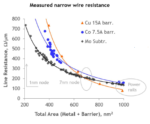
The figures below illustrate the relative comparison between these metals, as the dimensions are scaled with advancing process lithography.
Figure 2. Comparison of the resistivity of different metals with dimensional scaling, as a function of the cross-sectional area.
Note that damascene-based patterning at these dimensions will result in more impactful metal grain boundary influence on the electron mobility. Yet, Cu still outperforms the other metal options evaluated for large cross-sectional area.
Figure 3. Comparison of the via resistance of different metals.
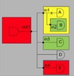
The DTCO team analyzed several different GAA-based cell topologies, evaluating their PPA characteristics. (Models for a three-layer GAA device with 13nm channel length and varying widths were developed by the team – these models were then applied for the cell design analysis.) The figure below depicts the six topologies considered.
Figure 4. Cell design alternatives.
The DTCO experiment parameters included:
- Evaluating Cu vs. Mo for signal wires (10nm wide, 20nm pitch)
- Adjusting GAA nanosheet device widths
- Exploring different cell track height options (5T, 5.5T, 6T, 6.5T, 20nm pitch)
- Defining multiple PDN options:
- Wide Cu power rails (larger cell size, less second metal stitching density required, measured as a multiple of the contacted poly pitch)
- Narrow Cu power rails (much tighter second metal stitching required)
- Thicker Cu power rails w/Mo signal wires (requiring a unique process to combine multiple metallurgies and extend the signal wire metal vertically)
- Introducing Mo buried power rails, with (optional) connectivity to smaller Cu power rails in the cell
The figure below details the four options A, B, C, and D. Options A and B continue to use Cu as the metallurgy. Designs C and D use thicker Cu for power rails, with additional processing to introduce a different metal for signal wires.
Figure 5. DTCO analysis cell design options, maintaining Cu as the power rail metallurgy. C and D use a “deeper” Cu power rail. The figure includes an additional VLSI 2020 Symposium reference that describes the process for incorporating composite interconnects for power (Cu) and signal wires (Co), as in options C and D.
The figure below illustrates the cell design incorporating a buried power rail (BPR), with Mo (or Ru) as the metallurgy.
Figure 6. DTCO analysis design options incorporating a buried power rail (Mo or Ru metallurgy).
An important facet to this analysis is the need to pursue the physical implementation of a large, complex block design, to evaluate: local pin access issues, overall routability (with the requisite PDN stitching density), power, and performance. The DTCO team completed the design of a GPU core for the six cell library options. The PPA results are shown below (as iso-power) – the 6T cell design serves as the baseline (“B”, 120nm tall, Cu signal wires, dense 30nm Cu power rails).
Figure 7. DTCO results for the six cell design options.
The “champion” of this PPA optimization analysis is configuration “C” – a 6T cell (120nm high) with a “deep” Cu first metal power rail and an alternative metallurgy for signal wires.
Note that the cost of the additional steps to provide for a composite metallurgy at first metal is not included in the analysis, nor were the steps to introduce the buried power rails.
I found the result to be of interest, as it demonstrates the significance of DTCO analysis. At advanced process node dimensions, the choice of (damascene or subtractive etch) metallurgies, the requisite patterning, and the GAA device design width are all strongly interrelated.
Of particular note were the results of the BPR cell designs, “E” and “F”. Note that the GPU block design area was minimal for these choices, suggesting that this may be the best option for embedded SRAM arrays. (Indeed, another presentation at VLSI 2020 provided a compelling argument for the bit cell area reductions afforded by using BPR for ground distribution, with VDD remaining on first metal.)
It will be intriguing to see how the foundries and their customers address the varied material and patterning DTCO options for sub-5nm nodes, for logic, SRAM, I/O’s, and mixed-signal IP. Of course, cost will be another critical factor in the ultimate selection. For more information on the Synopsys DTCO flows and these recent results, please follow this link.
-chipguy
References
[1] Moroz, V., et al., “Can We Ever Get to a 100nm Tall Library? Power Rail Design for 1nm Technology Node”, VLSI Symposium on Circuits and Technology 2020, paper JFS3.2.
Images supplied by the VLSI Symposium on Technology & Circuits 2020.
Also Read:
Webinar: Optimize SoC Glitch Power with Accurate Analysis from RTL to Signoff
The Problem with Reset Domain Crossings
What’s New in CDC Analysis?