IDC has forecasted that over the next five years, the Global Datasphere — the amount of data that’s created, transferred over the network and stored each year — will increase by over 3X to 175 zettabytes (Figure 1). Much of this is driven by the Internet of Things (IoT), video applications (including video streaming, social media, online gaming, augmented and virtual reality applications), and unified communications for video conferencing, text/chat and online voice communications.
Figure 1: Dramatic increase in the amount of network data that’s created, transferred, and stored
All of this data growth is driving the need for more compute power to process data in the cloud and high-performance computing (HPC) systems. To deliver the best experience at the endpoint, systems need faster interfaces to move data from point A to point B, an efficient and high performance storage infrastructure to store and retrieve data, and artificial intelligence (AI) and graphics accelerators to extract meaning from all of this data. High-performance IP can accelerate the design of chips that address these challenges.
Every HPC and cloud application has its own level of latency sensitivity, but they share three major sources of latency.
Latency Source 1: Network Latency
The first major source of latency is the network itself, including the time to move data between two points. Network latency is impacted by the distance that data must move. For example, with all else being equal, it’s much faster to move data between two nearby buildings than to move it across a continent.
Network latency is also impacted by the number of hops or network devices that the data has to traverse (which is typically directly related to the distance travelled). Minimizing the network distance and the number of hops can help to reduce network latency. To this end, cloud, telecom, and co-location service providers have recently established partnerships to put the power of cloud computing at the edge of the network, closer to the user and to end-user devices.
This helps to minimize latency and converge the data and services closer to the point of use for a much more responsive experience. It delivers smoother and more realistic experiences in applications like video streaming, augmented and virtual reality, and online gaming. (See How AI in Edge Computing Drives 5G and the IoT for a case study on this topic.)
In addition, moving cloud computing closer to the edge accelerates the response time for control system applications. In an automotive application, for example, a car moving at 60 miles per hour travels nearly 9 feet in 100 milliseconds – a blink of the eye. Any delay in data moving from the car to and from the cloud can be life-threatening. Offering nearly instantaneous response times gives the control system greater precision for increased safety.
Latency Source 2: Storage Latency
A second source of latency is the storage and retrieval of data, including the access time of the media. Historically, magnetic hard disk drives (HDDs) were the primary long-term data storage medium. HDDs had access times that were measured in milliseconds. But as solid state drives (SSDs) and persistent memory proliferate, media access time is measured in hundreds of nanoseconds, resulting in a 10,000X improvement in responsiveness (Figure 2).
Figure 2: As applications move from HDDs to persistent memory, systems see a 10,000x improvement in storage latency
The tremendous improvement in storage access times has resulted in network performance becoming the limiting factor for latency in a storage area network. Moving the storage closer to the CPU helps, as does using architectures such as persistent memory and innovative protocols like remote direct memory access (RDMA) to help accelerate storage transactions.
Another emerging technology in the storage space is computational storage. Computational storage combines compute capabilities with storage systems to offload computation or consumption of compute cycles from application servers. Computational storage allows processing to happen within the storage itself, reducing network traffic on the storage network and providing faster responses in certain applications.
Finally, smart network interface cards (NICs) are being adopted to reduce the load on application processors as data is transferred across the storage network. By offloading data transfer protocols, security protocols, and network management tasks from the application processor, smart NICs improve overall system performance for networked applications.
Latency Source 3: Compute Latency
The third source of latency is the actual compute time associated with data processing. The compute cycles and the movement of data between compute modules–between memory and the compute device–all impact data processing time. To address processing latency, designers need to address the amount of bandwidth available and the speed of the data transfer protocols.
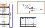
Figure 3 shows an example of two chips: a cloud server system-on-chip (SoC), which provides the application compute processing, and a graphics accelerator chip. The graphics accelerator uses HBM memory, and the cloud server chip uses traditional DDR memory. By utilizing a cash coherent interface between these two devices, the memory can be pooled in what we call a “converged memory pool” and the devices can share memory space without actually having to copy data from one process or domain to the other. This type of connection benefits from high-performance interface IP such as PCI Express 5.0, Compute Express Link (CXL), and Cache Coherent Interconnect for Accelerators (CCIX).
Figure 3: Cache coherent interfaces reduce compute latency
PCIe 5.0, CXL, or CCIX for Lowest Latency & Right Feature Set?
While low latency is the goal in cloud environments for fast processing of complex workloads, each protocol provides additional unique features and functionality that best fit the needs of the target application. Traditionally, servers relied on CPUs and storage for compute resources, which is no longer an option for today’s large hyperscale data centers with AI accelerators. A cloud server with a certain amount of memory, AI acceleration, GPUs, and networking capabilities, may require two CPUs and four storage devices or one storage device and two CPUs to process a particular workload. Each of these scenarios poses a different server configuration requirement for flexibility and scalability while continuing to focus on the goal of low latency. Let’s now examine the crowded field of low latency and cache coherent protocols to make it easier for designers to select the technology that best addresses their unique design needs.
While the market is preparing for PCIe 6.0, which is expected to be introduced in 2021, the shift from 16 GT/s PCIe 4.0 to PCIe 5.0 operating at 32 GT/s is quickly ramping up. A quick survey of our current Synopsys DesignWare® IP users shows many designs have already adopted the 32 GT/s PCIe 5.0 interface for their HPC applications. However, with the use of AI accelerators requiring more efficient memory performance, cache coherency combined with high bandwidth has become a critical demand. The CXL and CCIX protocols address this demand by reducing the amount of back and forth copying of data from the memory to processors and accelerators, dramatically lowering latency.
To fully optimize a system, selecting the right interface becomes critical to making the necessary tradeoffs between bandwidth, latency, memory access, topology, and implementation.
PCI Express
PCIe is the de-facto standard for chip-to-chip connectivity between the host and device. A simplified PCIe implementation can be between a PCIe root port (or root complex), and a PCIe endpoint through a four-lane (x4) link. A typical chip-to-chip PCIe implementation is expandable and hierarchical with embedded switches or switch chips that allow one root port to interface with multiple endpoints. Such an implementation is seen in laptops or even servers, allowing connectivity with different endpoints like Ethernet cards, display drivers, disk drives and other storage devices. However, the limitation of this implementation is seen in large systems with isolated memory pools that require heterogeneous computing where the processor and accelerator share the same data and memory space in a single 64-bit address space. In other words, the lack of a cache coherency mechanism in PCIe makes memory performance inefficient and latency less than acceptable as compared to some of the newer protocols like CXL and CCIX.
It is possible to leverage PCIe with what can be referred to as private links to enable data centers with servers that require chip-to-chip communication for multi-processing or between a processor and multiple accelerators. Private PCIe links can be used when both ends of a chip-to-chip link are owned by the same vendor, as parts of a typical PCIe data stream can be co-opted to help route information from chip to chip, outside of the PCIe protocol itself. Overloading the PCIe header and flexible new packets via vendor-defined messages enable messages to reach the intended chip in the chain. While this is not a typical implementation, many Synopsys users have adopted it.
CCIX
When CCIX was announced, it offered 20 GT/s and 25 GT/s data rates, which at the time was higher than PCIe 4.0 at 16GT/s, and the protocol added coherency capabilities. Today, CCIX v1.1 offers data rates up to 32GT/s and supports cache coherency, enabling multiple chips to share memory via a virtual memory space. Components that are connected in a single system become part of a large memory pool, eliminating the need to transfer large amounts of data between the processor and accelerator. CCIX enables heterogeneous computing with the ability to support mesh architectures where many CPUs or accelerators are interconnected and share data coherently.
While a CCIX implementation is very similar to PCIe, it implements two virtual channels (VCs): one each for the coherent and non-coherent traffic, resulting in latency on the order of PCI Express or slightly higher, which may not be appealing for HPC applications. Since CCIX is a symmetric protocol, every device in a CCIX implementation behaves the same and leverages a Home Agent where caching is managed. Due to the inherent symmetry, a coherency issue in any device can be detrimental to the entire system and not just the SoC.
CXL
CXL is ideal for host-to-device heterogeneous computing with support anticipated from all four CPU providers – Intel, IBM, Arm, and AMD. Unlike CCIX, CXL is an asymmetric protocol giving the host exclusive control of memory coherency and memory access. The advantages are a much simpler implementation of CXL devices, without the need for the Home Agent, which means that any mishandling of memory by a device will not cause system failure.
CXL runs across the PCIe physical layer, which is currently the PCIe 5.0 protocol operating at 32 GT/s. It uses a flexible processor port that can auto-negotiate a high-bandwidth CXL link, for example a x16 link, seamlessly plugging into either a PCIe or CXL card. Merging IO (.io), cache (.cache), and memory (.mem) protocols into one, CXL enables high bandwidth with an extremely low-latency interface, allowing the processor and accelerator to leverage a converged memory space. A converged memory space allows different memories such as HBM for the accelerator and DDR for the processor to be shared coherently. The required CXL.io protocol is effectively a PCIe link, and is used for discovery, register access, configuration of the link, and link bring up, while the .cache and .mem protocols are used for low-latency coherent data exchange, and one or both must be implemented to create a complete CXL link.
CXL delivers much lower latency than PCIe and CCIX by implementing the SerDes architecture in the newest PIPE specification, essentially moving the PCS layer, and its associated latency, from inside the PHY to the controller and allowing the CXL.cache and CXL.mem traffic to split from the CXL.io traffic very early in the stack. This combines with the inherent low latency of the CXL stack to give CXL lower latency than either PCIe or CCIX.
The three CXL protocols can be combined to create three distinct device types. Since the CXL.io protocol is mandatory it is implemented in all device types.
A Type 1 device implements CXL.io and CXL.cache protocols to allow attached devices like accelerators and smart NICs to cache and coherently access the host cache memory.
A Type 2 device implements all three protocols: CXL.io, CXL.cache, and CXL.mem to process the coherent data between the host and device-attached memory to optimize performance for a given task, allowing the Device to cache the Host memory and the Host to access attached device memory within a unified memory space.
Type 3 devices, such as memory expanders, are a very interesting implementation for HPC applications leveraging CXL.io and CXL.mem to allow the Host processor to access attached Device memory as if it were part of its own memory space.
Use cases for CXL Type 1 and 2 devices are applications that leverage accelerators, graphics, and computational storage. Use cases for Type 3 devices are applications that require storage class memory (persistent memory) and DDR that potentially will work over CXL. Replacing DDR controllers with CXL links is a new use case which the industry is exploring, leveraging the coherent memory access capabilities of CXL to make the SoC and board design less complex, versus using additional DDR memory. Another emerging application for CXL is the use of the CXS interface as an alternative to the separate CXL.cache and CXL.mem protocols. This approach can enable things like CCIX over CXL, potentially allowing support for a mesh network architecture and symmetric operation using the CCIX protocol, but over the low latency CXL link. This CCIX over CXL approach, using the CXS interface, enables links between multiple SoCs using CCIX while benefiting from the extremely low-latency provided by CXL.
Comparing the Three Interfaces
The PCIe interface is the de-facto standard for external connectivity in a wide range of applications including HPC. The ecosystem has developed and adopted new alternative protocols such as CCIX and CXL that leverage the PCIe physical layer and add several additional benefits like cache coherency and low latency. When selecting the right protocol, designers must make several trade-offs to best fit the needs of their target applications. Table 1 summarizes the unique characteristics of each protocol.
Table 1: Unique characteristics of PCIe, CXL, and CCIX best suited for HPC designs
While maximum bandwidth is the same across the three protocols, CXL offers the best latency at lower than 40 nanoseconds round trip by implementing the SerDes architecture and a CXL design from the ground up. Because CCIX is a symmetric protocol with support for mesh architecture, it adds connectivity for multiple accelerators. PCIe typically transfers a large block of data through a direct memory access (DMA) mechanism whereas CXL uses a dedicated CXL.mem protocol for short data exchanges and extremely low latency. Very similar to PCIe, CCIX uses a dedicated memory mechanism through two channels – coherent channel through VC1 and non-coherent channel through VC0.
The ecosystem has successfully adopted PCIe for a long time and understands its complexity and ways to manage it. CCIX adds the additional complexity of requiring a controller that supports two VCs and the required implementation of a Home Agent in every CCIX SoC, however, it offers slightly lower latency than PCIe and support for cache coherency. CXL adds the complexity of requiring a new controller, more interfaces, and more pins, however, it offers even lower latency than PCIe and CCIX in addition to cache coherency. PCIe, over five generations with PCIe 6.0 in the near future, has been proven and interoperated with third-party products. The newest interface, CXL, is being rapidly adopted by the industry with products expected in 2021. Intel has already announced their future Xeon Scalable processor with CXL support. CCIX, while introduced ahead of CXL, has been on a slow adoption path by the industry due to CXL’s more efficient memory access mechanism and low latency.
Conclusion
While each HPC SoC and cloud system has its own challenges and requirements, they all face compute latency, storage latency, and network latency. Understanding the latest interface IP standards that are available, along with their benefits and tradeoffs, can help designers minimize latency while integrating features that make their SoCs and systems stand above the competition.
Synopsys has delivered PCIe IP solutions to thousands of successful designs across the five generations of standards. For example, Synopsys recently announced and demonstrated the industry’s first DesignWare PCI Express 5.0 IP Interoperability with Intel’s Future Xeon Scalable Processor. In addition, Synopsys’ collaboration with Intel on CXL allowed us to deliver the industry’s first DesignWare CXL IP solution, including controller and 32GT/s PHY. We are working with other CPU vendors to support new applications using DesignWare CCIX and CXL IP for latency-optimized cloud and HPC solutions.
For more information:
DesignWare IP for HPC & Cloud Computing SoCs
DesignWare IP for PCIe
DesignWare CCIX IP
DesignWare CXL IP
Authors:
Scott Durrant, Strategic Marketing Manager, and Gary Ruggles, Sr. Product Marketing Manager, Synopsys
Also Read:
USB 3.2 Helps Deliver on Type-C Connector Performance Potential
Synopsys is Enabling the Cloud Computing Revolution
Synopsys Delivers a Brief History of AI chips and Specialty AI IP