Equalizers were initially designed and developed for movie theaters and amphitheaters or outdoor areas but now they have become ubiquitous. Equalization is essential for creating professional sound and creating real life like sound effects. Equalizers are used for controlling the energy/loudness of a particular frequency or a specific frequency range/band within an audio signal.
Introduction
Each musical note contains multiple frequencies. The base note of the instrument will be the ‘Fundamental Frequency’ and all the other frequencies in that particular musical note would be the ‘Harmonics’ of the ‘Fundamental Frequency’. The existence of these harmonics is what causes the sounds of instruments, to differ. Hence, a change in the Equalizer triggers a change in sounds.
The Equalizer is usually used as an element of audio post-processing. Once Audio Processing is implemented on a PCM signal, a post-processing algorithm (for e.g. an equalizer) can be provided for quality enhancements in the audio signal to increase listening pleasure.
Most home audio systems may have 5, 7 or 10 band equalizers. Professional music equipment uses 20 to 30 band equalizers.
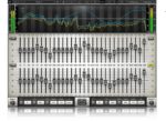
Figure 1: The Graphic Equalizer (Courtesy: https://www.waves.com/plugins/geq-graphic-equalizer)
Types of Equalizers
Graphic Equalizers: Graphic equalizers are the most commonly used equalizers for music systems. It works by allocating a range of frequencies in certain number of bands. The energy in the frequency bands are either attenuated, or boosted, depending on the requirement. The more the number of bands, the more the precision, and vice versa. However, they do not allow control over the shape of the filter for each band. Audio Filters are used to isolate bands, usually in a bell shape around the center frequency.
Parametric Equalizers: These are the most frequently used equalizers in high-end home audio systems and in some recording studios as well. The Parametric Equalizer lets you to control the Center Frequency, its Gain and the Range of each frequency band.
Dynamic Equalizers: This equalizer provides all the facilities given by the parametric equalizers and on top of that provide the user with the control of compression and expansion of an audio signal.
Shelving Equalizers: A shelving equalizer works similar to a High Pass or a Low Pass Filter. Here, the frequencies in the higher or lower end of the spectrum are boosted or attenuated. The boost or attenuation of frequencies is independent of center frequency for a Shelving filter.
Equalizer Fundamentals
In an Equalizer, the audio filters are used to isolate bands around the center frequency, usually, in a bell shape (Band Pass Filter). Analyzing the individual bands of an Equalizer (EQ) yields the filter characteristics of that particular EQ. These are important parameters as they help establish the spectral range in which an equalizer will operate (affect the sound). The filter characteristics are classified into:
Center Frequency: The center frequency for a band establishes the frequency around which the boost or cut in the sound energy affects the audio signal.
Filter Type: Filter Type determine the general shape of the EQ band. The most common filter types that used to design an Equalizer are High Pass Filter (HPF), Low Pass Filter (LPF), Notch Filter, High Shelf Filter (HSF) and a Low Shelf Filter (LSF)
Filter Slope: The slope of a filter indicates the rate of attenuation of sound beyond the cut-off frequency. The filter slope is a term usually associated with band pass, high pass and low pass filters.
Filter Q: It helps determine the bandwidth of a filter band. Q is known as the Quality Factor of an EQ.
Filter Gain: The filter gain is measured in dB (deciBels) and indicates the amount of boost or cut that is applied to a frequency band.
The Architecture of a Typical Equalizer
Almost all modern equalizers are based on Octave based Center Frequencies and use a ‘Frequency Warped’ filter design (i.e. the center frequencies are not equidistant) to minimize the inter-band frequency interference. This results in a smooth transition between bands. The most commonly used Audio EQ has been designed by Robert Bristow-Johnson (RBJ). The RBJ EQ too uses frequency warped time varying digital filters. In a time varying digital filter the filter coefficients change over time. Care must be taken to design the filter coefficients to avoid any noticeable artifacts due to the changing filter coefficients. Switching between one filter response to the other, instantaneously, causes unwanted artefacts in the audio output, hence output crossfading is applied to the nearby bands to reduce the artifacts. Crossfading requires the signal to be filtered with both the old and the new filters in parallel for consecutive bands. Thereafter, to smoothen out the transition in the waveform time-domain based crossfading is applied. The goal of crossfading is to keep the difference between bands to less than 3 dB.
The RBJ filter is an implementation of 2nd order filters with octave based bandwidth. Since it is an octave based filter, the bands can be divided only w.r.t the octave frequencies, (i.e. 1/3 Octaves or 2/3 Octaves or 1 octave or 2 octaves and so on) and the number of band of the EQ are dependent on the same.
RBJ Cook Book formulae for designing an EQ
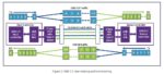
A second order filter is also known as a Biquad Filter. The Transfer function for a digital biquad filter (contains two poles and two zeros)
The above equation contains six coefficients. (namely: a0,a1,a2,b0,b1, and b2) The coefficients for the above equation are usually normalized such that a0 = 1. Now we have only 5 coefficients to work with. Since this is an IIR filter, the quantization error in coefficients can lead to instability. To avoid that cascaded second order filters are used in the design. For the filter to be stable, in the Z-domain, all the poles must be inside the unit circle.
Direct Form 1 implementation is typically used for implementing the above transfer function.
Figure 2: Digital Biquad Filter (Image Courtesy: https://en.wikipedia.org/wiki/Digital_biquad_filter)
Using the following “User defined” parameters the appropriate filters can be designed for an EQ.
Fs Sampling Frequency of Audio Signal
fc Center Frequency of the band
dBGain Used for Peaking and Shelving Filters
Q The Quality Factor
The coefficients for various filters are calculated using the above data and the RBJ cookbook formulae given below:
Low Pass Filter: (This filter removes all the frequencies above a specified frequency. It lets all the low frequencies to pass through and attenuates the higher frequencies)
High Pass Filter: (Removes all the frequencies below a specified frequency. It lets all the high frequencies to pass through and attenuates the lower frequencies)
Band Pass Filter: (Removes all the frequencies above and below specified cut-off frequencies. It only lets the frequencies in a particular band with a lower cut-off and higher cut-off frequency to pass through, and attenuates the frequencies outside the specified band)
Notch Filter: (These work on a very narrow band of frequencies. Removes all the frequencies in a narrow band. Notch filters are a subset a Band-Stop filters, with a very narrow band)
Peaking Filter: (A Peaking filter is used to boost or attenuate a range of frequencies around specified frequencies, to form a bell shape, by a ‘user defined’ value)
Low-Shelf Filter: (A Low-Shelf Filter is used to boost or attenuate a range of frequencies below the specified frequency, by a ‘user defined’ value)
High-Shelf Filter: (A High-Shelf Filter is used to boost or attenuate a range of frequencies above the specified frequency, by a ‘user defined’ value)
Where:
A (gain) = sqrt( 10^(dBgain/20) ) = 10^(dBgain/40) (for peaking and shelving EQ filters only) w0 (Angular freq) = 2*pi*fc/Fs
alpha = sin(w0)/(2*Q)
Once the coefficients are calculated using the above formulae, appropriate filter functions are called for each band. Usually, Shelving filters (Low-Shelf/High-Shelf) are used for the first and the last band of the EQ and Peaking filters (Bell Filters) are used for all the filters lying in between.
*These are just the fundamental building blocks of an equalizer and in no-way sufficient for designing the equalizer in totality.
Conclusion
Understanding the basics of filter shapes in an equalizer is fundamental to mix or create appropriate sound effects. One needs to know how to use an equalizer properly to make one’s own curves to change the way in which music and movies are heard, completely. Most home audio systems use simple filters for controlling/adjusting bass (low/very low frequencies), mid-range, and treble (high frequencies). When it comes to recording studios, the equalizers tend to be more sophisticated and are capable of finer adjustments. These high-end equalizers are capable of eliminating unwanted noise/sounds, and either suppress certain musical instruments or magnify particular frequencies to make some instruments sound more spectacular.
eInfochips is a CMMi Level 3 & ISO 9001:2008 certified Product Engineering Services company. We at eInfochips create value across the Software Development Life Cycle(SDLC) by providing DSP Middleware Software Development, Porting, Optimization, Support, and Maintenance services for various RISC and CISC SoC’s. We help our customer’s set-up Offshore Development Centers, supplementing the right teams and appropriate execution Models. For more information contact us today.
About the Author
Rhishikesh Agashe holds nearly 19 years of experience in the IT Industry. 4 years as an Entrepreneur and 15 years in the Embedded domain wherein most of his experience was in Embedded Media Processing where he was involved in Implementation of Audio and Speech Algorithms on various Microprocessors/DSPs(ARM/MIPS/TI/CRADLE/CevaDSP/Meta).
References:
- https://www.musicdsp.org/en/latest/_downloads/3e1dc886e7849251d6747b194d482272/Audio-EQ-Cookbook.txt
- https://en.wikipedia.org/wiki/Digital_biquad_filter
Also read:
Understanding BLE Beacons and their Applications
Sign Off Design Challenges at Cutting Edge Technologies
Techniques to Reduce Timing Violations using Clock Tree Optimizations in Synopsys IC Compiler II