The term von Neumann bottleneck is used to denote the issue with the efficiency of the architecture that separates computational resources from data memory. The transfer of data from memory to the CPU contributes substantially to the latency, and dissipates a significant percentage of the overall energy associated with the computation.
This energy inefficiency is especially acute for the implementation of machine learning algorithms using neural networks. There is a significant research emphasis on in-memory computing, where hardware is added to the memory array in support of repetitive, vector-based data computations, reducing the latency and dissipation of data transfer to/from the memory.
In-memory computing is well-suited for machine learning inference applications. After the neural network is trained, the weights associated with the multiply-accumulate (MAC) operations at each network node are stored in the memory, and can be used directly as multiplication operands.
At the recent International Solid-State Circuits Conference (ISSCC), researchers from the National Tsing Hua University and TSMC presented several novel design implementation approaches toward in-memory computing, using resistive RAM (ReRAM). [1] Their techniques will likely help pave the way toward more efficient AI implementations, especially at the edge where latency and power dissipation are key criteria.
Background
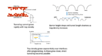
An example of a fully-connected neural network is shown in the figure below.
A set of input data (from each sample) is presented to the network – the input layer. A series of computations is performed at each subsequent layer. In the fully-connected network illustrated above, the output computation from each node is presented to all nodes in the next layer. The final layer of the trained network is often associated with determining a classification match to the input data, from a fixed set of labeled candidates (“supervised learning”).
The typical computation performed at each node is depicted below. Each data value is multiplied by its related (trained) weight constant, then summed – a multiply-accumulate (MAC) calculation. A final (trained) bias value may be added. The output of a numeric activation function is used to provide the node output to the next layer.
The efficiency of the node computation depends strongly on the MAC operation. In-memory computing architectures attempt to eliminate the delay and power dissipation of transferring weight values for the MAC computation.
The figures above illustrate how the multiplication of (data * weight) could be implemented using the value stored in a one-transistor, one-resistor (1T1R) ReRAM bitcell. [2]
ReRAM technology offers a unique method for non-volatile storage in a memory array. A write cycle to the bitcell may change the property of the ReRAM material, between a high-resistance (HR) and low-resistance (LR) state. Subsequent to the write cycle, a bitline current-sense read cycle differentiates between the resistance values to determine the stored bit.
Again referring to the figure above, with the assumption that HR = ‘0’ and LR = ‘1’, the ReRAM cell implements the (data * weight) product in the following manner:
- if the data = ‘0’, the word line to the bitcell is inactive and little bitline current flows
- if the data = ‘1’ (word line active), their bitcell current will either be iHR or iLR
If the bitline current sense circuitry distinguishes between iHR (small) and iLR (large), only the product (data = ‘1’) * (weight = ‘1’) = ‘1’ results in significant bitline current.
The summation of the (data * weight) product for multiple data values into the fully-connected network node is illustrated in the figure above. Unlike a conventional memory array where only one decoded address word line is active, the in-memory computing MAC will have an active word line for each node input where (data = ‘1’). The total bitline current will be the sum of the parallel ‘dotted’ bitcell currents where the individual word lines are active, either iLR or iHR for each. The multiply-accumulate operation for all (data * weights) is readily represented as the total bitline current.
At the start of the MAC operation, assume a capacitor connected to the bitline is set to a reference voltage (say, either fully pre-charged or discharged). The clocked duration of the MAC computation will convert the specific bitline current in that clock cycle into a voltage difference on that capacitor:
delta_V = (I_bitline) * (delta_T) / Creference
That voltage can be read by an analog-to-digital converter (ADC), to provide the digital equivalent of the MAC summation.
In-Computing ReRAM Innovations
The ISSCC presentation from researchers at National Tsing Hua University and TSMC introduced several unique innovations to the challenges of ReRAM-based in-memory computing.
Data and Weight Vector Widths
The simple examples in the figures above used a one-bit data input and a one-bit weight. A real edge AI implementation will have data vector and weight vector widths as input to the MAC operation. For example, consider the case of 8-bit data and 8-bit weights for each multiplication product in the MAC operation. (Parenthetically, the vector width of the weights after network training need not be the same of the input data vector width. Further, the numeric value of the width vector could be any of a number of representations – e.g., signed or unsigned integer, twos complement.) For the example, at each network node, the in-memory computation architecture needs to compute multiple products of two 8-bit vectors and accumulate the sum.
While the ReRAM array macro computes the MAC for the network node, circuitry outside the array would be used to add the bias, and apply the activation function. This function would also normalize the width of the node output result to the input data vector width for the next network layer.
The researchers implemented a novel approach toward the MAC calculation, expanding upon the 1-bit ReRAM example shown above.
The description above indicated that the duration of the bitline current defines the output voltage on the reference capacitor.
The researchers reviewed several previous proposals for generating the data vector input-to-word line duration conversion, as illustrated below.
The input data value could be decoded into a corresponding number of individual word line pulses, as illustrated below.
Alternatively, the data value could be decoded into a word line pulse of different durations. The multiplication of the data input vector times each bit of the weight could be represented by different durations of the active word line to the ReRAM bit cell, resulting in different cumulative values of bitline current during the read cycle. The figure below illustrates the concept, for four 3-bit data inputs applied as word lines to a weight vector bitline, shown over two clock cycles.
For a data value of ‘000’, the word line would remain off; for a data value of ‘111’, the maximum word line decode pulse duration would be applied. The data input arcs to the network node would be dotted together as multiple active cells on the column bitline, as before.
Each column in the ReRAM array corresponds to one bit of the weight vector – the resulting voltage on the reference capacitor is the sum of all node data inputs times one bit of the weight.
Outside of the ReRAM array itself, support circuitry is provided to complete the binary vector (data*weight) multiplication and accumulation operation:
- an ADC on each bitline column converts the voltage value to a binary vector
- shifting the individual binary values for the MSB to LSB of the weight vector
- generating the final MAC summation of the shifted weight bits
The researchers noted that these two approaches do not scale well to larger data vector widths:
- the throughput is reduced, as longer durations are needed
- for the long pulse approach, PVT variations will result in jitter in the active word line duration, impacting the accuracy
The researchers chose to implement a novel, segmented duration approach. For example, an 8-bit data input vector is divided into 3 separate ReRAM operations, of 2-3-3 bits each. The cumulative duration of these three phases is less than the full data decode approach, improving the computation throughput.
Scaling the Bitline Current
With the segmented approach, the researchers described two implementation options:
- at the end of each phase, the reference capacitor voltage is sensed by the ADC, then reset for the next phase; the ADC output provides the data times weight bit product for the segmented data vector slice
- the reference capacitor voltage could be held between phases, without a sample-and-reset sequence
In this second case, when transitioning from one data vector segment to the next, it is necessary to scale the capacitor current correspondingly. If the remaining data vector width for the next segment phase is n bits, the capacitor current needs to be scaled by 1/(2**n). The figure below provides a simplified view to how the researchers translated the bitline current in each phase into a scaled reference capacitor current.
A pFET current mirror circuit is used to generate a current into the reference capacitor; the unique nature of a current mirror is by adjusting device sizes in the mirror branch, scaled values of the bitline current are generated. Between the data vector segment phases, the capacitor voltage is held, and a different scaled mirror current branch is enabled.
For the in-memory ReRAM computing testsite, the researchers chose to use the full reference capacitor reset phase for the most significant bits segment, to provide the optimum accuracy, as required for the MSBs of the data input. For the remaining LSBs of the data, the subsequent phases used the switched current mirror approach.
Process Variations
The researchers acknowledged that there are significant tolerances in the high and low resistance values of each ReRAM bitcell. When using ReRAM as a simple memory array, there is sufficient margin between lowR and highR to adequately sense a stored ‘1’ and ‘0’.
However, as the in-memory computing requirements rely on accumulation of specific (dotted) bitcell currents, these variations are a greater issue. The researchers chose to use an “averaging” approach – each stored weight bit value is copied across multiple ReRAM bitcells (e.g., # of copies = 4). Although the figures above depict each data input vector as one ReRAM word line, multiple word lines connected each weight bit are used.
Testsite and FOM
TSMC fabricated an ReRAM testsite using this segmented data vector technique. The specs are shown in the figure above. The testsite provided programmability for different data vector widths and weight vector widths – e.g., 8b-8b-14b represents an eight bit data input, an eight bit weight, and a full MAC summation supporting a fourteen bit result at the network node.
The researchers defined a figure-of-merit for MAC calculations using in-memory computing:
FOM = (energy_efficiency * data_vector_width * weight_vector_width * output_vector_width) / latency
(Energy efficiency is measured in TOPS/Watt; the output vector width from the ReRAM array and support circuitry is prior to bias addition and activation/normalization.)
Summary
Edge AI implementations are hampered by the power and latency inefficiencies associated with the von Neumann bottleneck, which has sparked great interest in the field of in-memory computing approaches. Read access to a ReRAM array storing weight values offers a unique opportunity to implement a binary product of data and weights. Researchers at TSMC and National Tsing Hua University have implemented several novel approaches toward the use of ReRAM for the MAC computation at each neural network node, addressing how to efficiently work with wide data vectors, and manage ReRAM process variation. I would encourage you to read their recent technical update provided at ISSCC.
-chipguy
References
[1] Xue, Cheng-Xin, et al., “A 22nm 4Mb 8b-Precision ReRAM Computing-in-Memory Macro”, ISSCC 2021, paper 16.1.
[2] Mao, M., et al., “Optimizing Latency, Energy, and Reliability of 1T1R ReRAM Through Cross-Layer Techniques”, IEEE Journal on Emerging and Selected Topics in Circuits and Systems, 2016, p. 352-363.