The introduction of heterogeneous 3DIC packaging technology offers the opportunity for significant increases in circuit density and performance, with corresponding reductions in package footprint. Yet, the implementation of a complex 3DIC product requires a considerable investment in methodology development for all facets of the design:
- system architecture partitioning (among die)
- I/O assignments for all die, both for signals and the power distribution network (PDN)
- die floorplanning, driven by the I/O assignments
- probe card design (with potential reuse between individual die and 3DIC assembly)
- critical timing path analysis, assessing the tradeoffs between timing paths on-die versus the implementation of vertical paths between stacked die
- IR drop analysis, a key facet of 3DIC planning due to the power delivery to stacked die using through-silicon or through-dielectric vias
- a DFT architecture, suitable for 3DIC testing using individual known good die (KGD)
- reliability analysis of the composite multi-die thermal package model
- LVS physical verification of the multi-die connectivity model
Whereas 2.5D IC packaging technology has pursued “chiplet-based” die functionality (and potential electrical interface connectivity standards), the complexity of 3DIC implementations requires early and extensive investment in the design and analysis flows listed above – a higher risk than 2.5D IC implementations, for sure, but with a potentially greater reward.
At the recent IEDM 2020 conference, TSMC presented an enlightening paper describing their recent efforts to tackle these 3DIC implementation tradeoffs, using a very interesting testchip implementation. This article summarizes the highlights of their presentation. [1]
SoIC Packaging Technology
Prior to IEDM, TSMC presented their 3DIC package offering in detail at their Technology Symposium – known as “System on Integrated Chip”, or SoIC (link).
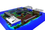
A (low-temperature) die-to-die bonding technology provides the electrical connectivity and physical attach between die. The figure below depicts available die attach options – i.e., face-to-face, face-to-back, and a complex combination including side-to-side assembly potentially integrating other die stacks.
For the face-to-face orientation, the backside of the top die receives the signal and PDN redistribution layers. Alternatively, a third die on the top of the SoIC assembly may be used to implement the signal and PDN redistribution layers to package bumps – a design testcase from TSMC using the triple-stack will be described shortly.
A through-silicon via (TSV) in die #2 provides electrical connectivity for signals and power to die #1. A through-dielectric via (TDV) is used for connectivity between the package and die #1 in the volumetric region outside of the smaller die #2.
Planning of the power delivery to the SoIC die requires consideration of several factors:
- estimated power of each die (especially where die #1 is a high-performance, high-power processing unit)
- TSV/TDV current density limits
- distinct power domains associated with each die
The figure below highlights the design option of “number of TSVs per power/ground bump”. To reduce IR drop and observe current density limits through a TSV, an array of TSVs may be appropriate – as an example, up to 8 TSVs are shown in the figure. (Examples from both FF and SS corners are shown.)
The tradeoff of using multiple, arrayed TSVs is the impact on interconnect density.
As an illustration, TSMC pursued a unique SoIC implementation – a quad-core ARM A72 processor (die #1) where the L2$ cache arrays commonly integrated with each core have been re-allocated to die #2. The CPU die in process node N5 maintains an L3$ array, while the SRAM die in process node N7 contains the full set of L2$ arrays. A third die on top of die #2 provides the redistribution layers. A total of 2700 connections are present between CPU die #1 and the L2$ arrays in die #2.
This is an example of how SoIC technology could have a major impact on system architectures, where a (large) cache memory is connected vertically to a core, rather than integrated laterally on a monolithic die.
PDN Planning
A key effort in the development of an SoIC is the concurrent engineering related to the assignment of bump, pad, and TSV/TDV locations throughout, for both signals and the PDN.
The figures above highlight the series of planning steps to develop the TSV configuration for the PDN – a face-to-face die attach configuration is used as an example. The original “dummy” bond pads between die (for mechanical stability) are replaced with the signal and PDN TDV and TSV arrays. (TSMC also pursued the goal of re-using the probe card, between die #1 testing and the final SoIC testing – that goal influenced the assignment of pad and TSV locations.)
The TSV implementations for the CPU die and SRAM die also need to be carefully chosen so as to meet IR goals, without adversely impacting overall die interconnect density.
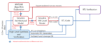
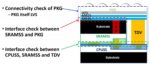
LVS
Briefly, TSMC also highlighted the (multi-phase) LVS connectivity verification methodology, and unique DFT architecture selected for this SoIC test vehicle, as depicted below.
DFT
Another major consideration is the DFT architecture for the SoIC, and how connectivity testing will be accomplished using cross-die scan, as illustrated below.
TSMC demonstrated that the resulting (N5 + N7) SoIC design achieved a 15% performance gain (with suitable L2$ and L3$ hit rate and latency assumptions), leveraging a significant reduction in point-to-point distance afforded by the vertical connectivity between die. The package areal footprint for the SoIC is reduced by ~50% from a monolithic 2D implementation.
3D SoIC packaging technology will offer system architects with unique opportunities to pursue design partitioning across vertical die configurations. The density and electrical characteristics of the vertical bond connections may offer improved performance over lateral (monolithic or 2.5D chiplet-based) interconnects. (The additional power dissipation of “lite I/O” driver and receiver cells between die versus on-chip signal buffering is typically small.)
The tradeoff is the investment required to develop the SoIC die floorplans for TSV and TDV vias to provide the requisite signal count and low IR drop PDN. Although 2.5D chiplet-based package offerings have been aggressively adopted, the performance and footprint advantages of a 3DIC are rather compelling. The TSMC test vehicle demonstrated at IEDM will no doubt generate considerable interest.
-chipguy
References
[1] Cheng, Y.-K., et al., “Next-Generation Design and Technology Co-optimization (DTCO) of System on Integrated Chip (SoIC) for Mobile and HPC Applications”, IEDM 2020.