
The Intel 8086 microprocessor was introduced 42 years ago last month,1 so I made some high-res die photos of the chip to celebrate. The 8086 is one of the most influential chips ever created; it started the x86 architecture that still dominates desktop and server computing today. By looking at the chip’s silicon, we can see the internal features of this chip.
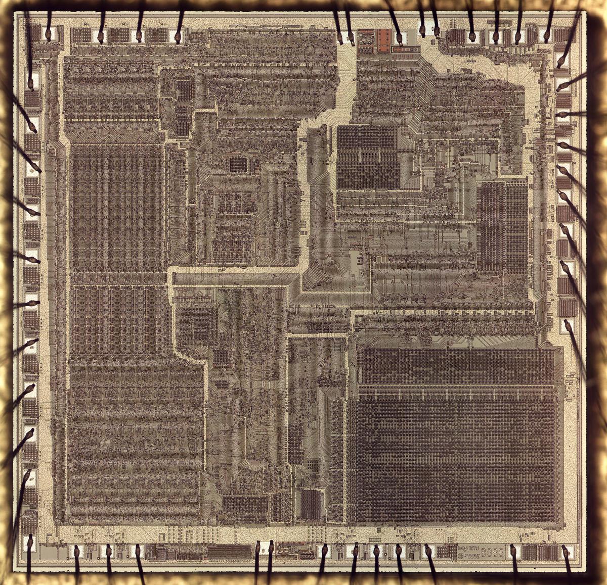
The photo below shows the die of the 8086. In this photo, the chip’s metal layer is visible, mostly obscuring the silicon underneath. Around the edges of the die, thin bond wires provide connections between pads on the chip and the external pins. (The power and ground pads each have two bond wires to support the higher current.) The chip was complex for its time, containing 29,000 transistors.

Looking inside the chip
To examine the die, I started with the 8086 integrated circuit below. Most integrated circuits are packaged in epoxy, so dangerous acids are necessary to dissolve the package. To avoid that, I obtained the 8086 in a ceramic package instead. Opening a ceramic package is a simple matter of tapping it along the seam with a chisel, popping the ceramic top off.

With the top removed, the silicon die is visible in the center. The die is connected to the chip’s metal pins via tiny bond wires. This is a 40-pin DIP package, the standard packaging for microprocessors at the time. Note that the silicon die itself occupies a small fraction of the chip’s size.

Using a metallurgical microscope, I took dozens of photos of the die and stitched them into a high-resolution image using a program called Hugin (details). The photo at the beginning of the blog post shows the metal layer of the chip, but this layer hid the silicon underneath.

For the die photo below, the metal and polysilicon layers were removed, showing the underlying silicon with its 29,000 transistors.2 The labels show the main functional blocks, based on my reverse engineering. The left side of the chip contains the 16-bit datapath: the chip’s registers and arithmetic circuitry. The adder and upper registers form the Bus Interface Unit that communicates with external memory, while the lower registers and the ALU form the Execution Unit that processes data. The right side of the chip has control circuitry and instruction decoding, along with the microcode ROM that controls each instruction.

One feature of the 8086 was instruction prefetching, which improved performance by fetching instructions from memory before they were needed. This was implemented by the Bus Interface Unit in the upper left, which accessed external memory. The upper registers include the 8086’s infamous segment registers, which provided access to a larger address space than the 64 kilobytes allowed by a 16-bit address. For each memory access, a segment register and a memory offset were added to form the final memory address. For performance, the 8086 had a separate adder for these memory address computations, rather than using the ALU. The upper registers also include six bytes of instruction prefetch buffer and the program counter.
The lower-left corner of the chip holds the Execution Unit, which performs data operations. The lower registers include the general-purpose registers and index registers such as the stack pointer. The 16-bit ALU performs arithmetic operations (addition and subtraction), Boolean logical operations, and shifts. The ALU does not implement multiplication or division; these operations are performed through a sequence of shifts and adds/subtracts, so they are relatively slow.
Microcode
One of the hardest parts of computer design is creating the control logic that tells each part of the processor what to do to carry out each instruction. In 1951, Maurice Wilkes came up with the idea of microcode: instead of building the control logic from complex logic gate circuitry, the control logic could be replaced with special code called microcode. To execute an instruction, the computer internally executes several simpler micro-instructions, which are specified by the microcode. With microcode, building the processor’s control logic becomes a programming task instead of a logic design task.
Microcode was common in mainframe computers of the 1960s, but early microprocessors such as the 6502 and Z-80 didn’t use microcode because early chips didn’t have room to store microcode. However, later chips such as the 8086 and 68000, used microcode, taking advantage of increasing chip densities. This allowed the 8086 to implement complex instructions (such as multiplication and string copying) without making the circuitry more complex. The downside was the microcode took a large fraction of the 8086’s die; the microcode is visible in the lower-right corner of the die photos.3

Bits are stored by the presence or absence of transistors. The transistors are the small white rectangles above and/or below each dark rectangle. The dark rectangles are connections to the horizontal output buses in the metal layer.
The photo above shows part of the microcode ROM. Under a microscope, the contents of the microcode ROM are visible, and the bits can be read out, based on the presence or absence of transistors in each position. The ROM consists of 512 micro-instructions, each 21 bits wide. Each micro-instruction specifies movement of data between a source and destination. It also specifies a micro-operation which can be a jump, ALU operation, memory operation, microcode subroutine call, or microcode bookkeeping. The microcode is fairly efficient; a simple instruction such as increment or decrement consists of two micro-instructions, while a more complex string copy instruction is implemented in eight micro-instructions.3
History of the 8086
The path to the 8086 was not as direct and planned as you might expect. Its earliest ancestor was the Datapoint 2200, a desktop computer/terminal from 1970. The Datapoint 2200 was before the creation of the microprocessor, so it used an 8-bit processor built from a board full of individual TTL integrated circuits. Datapoint asked Intel and Texas Instruments if it would be possible to replace that board of chips with a single chip. Copying the Datapoint 2200’s architecture, Texas Instruments created the TMX 1795 processor (1971) and Intel created the 8008 processor (1972). However, Datapoint rejected these processors, a fateful decision. Although Texas Instruments couldn’t find a customer for the TMX 1795 processor and abandoned it, Intel decided to sell the 8008 as a product, creating the microprocessor market. Intel followed the 8008 with the improved 8080 (1974) and 8085 (1976) processors. (I’ve written more about early microprocessors here.)

In 1975, Intel’s next big plan was the 8800 processor designed to be Intel’s chief architecture for the 1980s. This processor was called a “micromainframe” because of its planned high performance. It had an entirely new instruction set designed for high-level languages such as Ada, and supported object-oriented programming and garbage collection at the hardware level. Unfortunately, this chip was too ambitious for the time and fell drastically behind schedule. It eventually launched in 1981 (as the iAPX 432) with disappointing performance, and was a commercial failure.
Because the iAPX 432 was behind schedule, Intel decided in 1976 that they needed a simple, stop-gap processor to sell until the iAPX 432 was ready. Intel rapidly designed the 8086 as a 16-bit processor somewhat compatible with the 8-bit 8080,4 released in 1978. The 8086 had its big break with the introduction of the IBM Personal Computer (PC) in 1981. By 1983, the IBM PC was the best-selling computer and became the standard for personal computers. The processor in the IBM PC was the 8088, a variant of the 8086 with an 8-bit bus. The success of the IBM PC made the 8086 architecture a standard that still persists, 42 years later.
Why did the IBM PC pick the Intel 8088 processor?7 According to Dr. David Bradley, one of the original IBM PC engineers, a key factor was the team’s familiarity with Intel’s development systems and processors. (They had used the Intel 8085 in the earlier IBM Datamaster desktop computer.) Another engineer, Lewis Eggebrecht, said the Motorola 68000 was a worthy competitor6 but its 16-bit data bus would significantly increase cost (as with the 8086). He also credited Intel’s better support chips and development tools.5
In any case, the decision to use the 8088 processor cemented the success of the x86 family. The IBM PC AT (1984) upgraded to the compatible but more powerful 80286 processor. In 1985, the x86 line moved to 32 bits with the 80386, and then 64 bits in 2003 with AMD’s Opteron architecture. The x86 architecture is still being extended with features such as AVX-512 vector operations (2016). But even though all these changes, the x86 architecture retains compatibility with the original 8086.
Transistors
The 8086 chip was built with a type of transistor called NMOS. The transistor can be considered a switch, controlling the flow of current between two regions called the source and drain. These transistors are built by doping areas of the silicon substrate with impurities to create “diffusion” regions that have different electrical properties. The transistor is activated by the gate, made of a special type of silicon called polysilicon, layered above the substrate silicon. The transistors are wired together by a metal layer on top, building the complete integrated circuit. While modern processors may have over a dozen metal layers, the 8086 had a single metal layer.

The closeup photo of the silicon below shows some of the transistors from the arithmetic-logic unit (ALU). The doped, conductive silicon has a dark purple color. The white stripes are where a polysilicon wire crossed the silicon, forming the gate of a transistor. (I count 23 transistors forming 7 gates.) The transistors have complex shapes to make the layout as efficient as possible. In addition, the transistors have different sizes to provide higher power where needed. Note that neighboring transistors can share the source or drain, causing them to be connected together. The circles are connections (called vias) between the silicon layer and the metal wiring, while the small squares are connections between the silicon layer and the polysilicon.

Closeup of some transistors in the 8086. The metal and polysilicon layers have been removed in this photo. The doped silicon has a dark purple appearance due to thin-film interference.
Conclusions
The 8086 was intended as a temporary stop-gap processor until Intel released their flagship iAPX 432 chip, and was the descendant of a processor built from a board full of TTL chips. But from these humble beginnings, the 8086’s architecture (x86) unexpectedly ended up dominating desktop and server computing until the present.
Although the 8086 is a complex chip, it can be examined under a microscope down to individual transistors. I plan to analyze the 8086 in more detail in future blog posts8, so follow me on Twitter at @kenshirriff for updates. I also have an RSS feed. Here’s a bonus high-resolution photo of the 8086 with the metal and polysilicon removed; click for a large version.

Die photo of the Intel 8086 processor. The metal and polysilicon have been removed to reveal the underlying silicon.
Notes and references
- The 8086 was released on June 8, 1978. ↩
- To expose the chip’s silicon, I used Armour Etch glass etching cream to remove the silicon dioxide layer. Then I dissolved the metal using hydrochloric acid (pool acid) from the hardware store. I repeated these steps until the bare silicon remained, revealing the transistors. ↩
- The designers of the 8086 used several techniques to keep the size of the microcode manageable. For instance, instead of implementing separate microcode routines for byte operations and word operations, they re-used the microcode and implemented control circuitry (with logic gates) to handle the different sizes. Similarly, they used the same microcode for increment and decrement instructions, with circuitry to add or subtract based on the opcode. The microcode is discussed in detail in New options from big chips and patent 4449184. ↩↩
- The 8086 was designed to provide an upgrade path from the 8080, but the architectures had significant differences, so they were not binary compatible or even compatible at the assembly code level. Assembly code for the 8080 could be converted to 8086 assembly via a program called CONV-86, which would usually require manual cleanup afterward. Many of the early programs for the 8086 were conversions of 8080 programs. ↩
- Eggebrecht, one of the original engineers on the IBM PC, discusses the reasons for selecting the 8088 in Interfacing to the IBM Personal Computer (1990), summarized here. He discussed why other chips were rejected: IBM microprocessors lacked good development tools, and 8-bit processors such as the 6502 or Z-80 had limited performance and would make IBM a follower of the competition. I get the impression that he would have preferred the Motorola 68000. He concludes, “The 8088 was a comfortable solution for IBM. Was it the best processor architecture available at the time? Probably not, but history seems to have been kind to the decision.” ↩
- The Motorola 68000 processor was a 32-bit processor internally, with a 16-bit bus, and is generally considered a more advanced processor than the 8086/8088. It was used in systems such as Sun workstations (1982), Silicon Graphics IRIS (1984), the Amiga (1985), and many Apple systems. Apple used the 68000 in the original Apple Macintosh (1984), upgrading to the 68030 in the Macintosh IIx (1988), and the 68040 with the Macintosh Quadra (1991). However, in 1994, Apple switched to the RISC PowerPC chip, built by an alliance of Apple, IBM, and Motorola. In 2006, Apple moved to Intel x86 processors, almost 28 years after the introduction of the 8086. Now, Apple is rumored to be switching from Intel to its own ARM-based processors. ↩
- For more information on the development of the IBM PC, see A Personal History of the IBM PC by Dr. Bradley. ↩
- The main reason I haven’t done more analysis of the 8086 is that I etched the chip for too long while removing the metal and removed the polysilicon as well, so I couldn’t photograph and study the polysilicon layer. Thus, I can’t determine how the 8086 circuitry is wired together. I’ve ordered another 8086 chip to try again. ↩


Comments
6 Replies to “A Look at the Die of the 8086 Processor”
You must register or log in to view/post comments.