You are currently viewing SemiWiki as a guest which gives you limited access to the site. To view blog comments and experience other SemiWiki features you must be a registered member. Registration is fast, simple, and absolutely free so please, join our community today!
Today is SemiWiki’s 10th anniversary so an extra special Happy New Year to all! It has been an exciting 10 year adventure for sure and I hope it can continue for another 10 years, absolutely.
2020 brought in a record amount of content, readers and members. Our readership grew 70% YoY in 2020 according to Google Analytics which is a big number. Readership grew 15% YoY in 2019 which was about average. Total SemiWiki.com readers over the ten years are now more than 4 million with more than 50M blog views!
In 2020 the new SemiWiki job board attracted 395,943 views and the community calendar recorded 404,224 views. The new press release section recorded 1,480,953 views and the company wikis received an additional 158,743 views. We published 670 blogs that recorded more than 6M views, another SemiWiki record. Thankfully, SemiWiki 2.0 is easily scalable in the cloud, another handy 2020 addition.
For this amazing success we thank you all. What’s coming up for SemiWiki in 2021 you ask?
First and foremost, our new podcast series “Semiconductor Insiders” starting tomorrow Jan 2, 2021. This will be a weekly series hosted by myself and the top 2020 SemiWiki blogger Mike Gianfagna.
“The goal of this Podcast Series is to bring semiconductor experts together to get to the truth about the matter at hand. We’ll get right to the point and not exceed 30 minutes of your time. If you have a topic you would like us to cover please post it on SemiWiki.com and we will get right to it.”
Mike and I did the introductory EP1 which is titled “Why are Semiconductors so Sexy”. EP2 is “Moore’s Law Dead or Alive” with Dr. Walden Rhines. EP3 is “Tomorrow’s Semiconductors” with Jim Hogan and EP4 is “Can China Really Become Self-Sufficient in Semiconductors” with Robert Maire. February is still in the planning phase so submit your topics in the comments section.
Secondly, virtual events are so much easier for us to cover and I expect that to continue in 2021. More events, more expert coverage, more content for all. We are finishing up IEDM 2020 coverage this month and ISSCC is up next then SPIE and DVCon.
Thirdly, we added the SemiWiki Webinar Series in 2020 which was attended by thousands of people. Webinars are still the best virtual event for ROI in all regards. This year we will do more of the same with maybe a slight twist or turn.
Fourthly, the SemiWiki LinkedIn group now has more than 21,000 members. LinkedIn is our top social media channel so please join as my guest and support our community. SemiWiki also has a LinkedIn company page where we post relevant press releases from the semiconductor ecosystem. Please follow us there as well. If you want your press release or news event posted send it to admin at SemiWiki dot com.
Fifthly, something you all may not know, SemiWiki has internal email so members can connect and discuss topics at hand in private. A record number of email was sent this year and I expect that to continue since we cannot connect and network at live events.
Finally, here are the top ten most viewed blogs is 2020:
If you have ideas or suggestions on how SemiWiki can improve in 2021 for the greater good let me know via SemiWiki email. It would be a pleasure to speak with you.
This area of automating the design of Flat Panel Displays (FPD) is so broad that it has taken me three blogs to cover all of the details, so in brief review the first two blogs were:
The following Q&A is with Chen Zhao, from Empyrean, and he’s an AE that’s been with the company since 2014.
Q: IC designers use DRC and LVS tools, so how’s the process different with curvilinear FPDs?
The function of the layout verification tool is to check whether the layout meets the design rules and electrical rules, and whether the layout is consistent with the schematic diagram, etc. 1
It is essential for eliminating errors, reducing design costs and reducing the risk of design failure. General layout verification techniques are developed for rectangular layouts. The emergence of curvilinear-shaped designs poses a great challenge to the layout verification technology. It is necessary to develop new algorithms suitable for curvilinear-shaped designs based on traditional computational geometry algorithms 2, 3.
The grid is used in the layout to determine the position of the graphics, and the vertices of the graphics are on the grid points. The rotation of the layout may cause the vertices and grid points of the graphics to be misaligned, causing the two sides that were originally perpendicular to be no longer perpendicular. Take the next figure as an example. After rotation, “a” and “c”, and “a” and “e” no longer maintain 90 degrees, DRC may report false errors, such as the minimum distance for “a-c” or “d-e” is not enough. At this time, it is necessary to add support angle tolerance rules, by filtering out errors with features such as “small edges” and “small corners” to avoid false errors. Of course, this method has certain risks. The user can output these errors to a specific file to distinguish these minor errors from important errors and check important errors first.
In addition, if you can merge the graphics before rotation, you can also avoid errors.
Layout rotation causes false DRC error
Due to the rotation of the layout, the error increases. LVS may cause the device extraction failure when extracting the circuit netlist.
An MOS transistor example, after rotation, the source and drain terminals do not intersect with the gate due to the dislocation of the vertices and grid points, and the transistor extraction fails. The above DRC methods to eliminate false errors, such as supporting tolerance, merging before graphics rotation, etc., are also applicable to LVS.
Layout rotation causes false LVS error
ArgusFPD parallel hierarchical layout verification tool developed by Empyrean focuses on the FPD market. It faces the verification needs of ultra-large-scale layouts and advanced design methods such as curvilinear-shaped designs. It provides customers with layout verification solutions that can meet the needs of FPD design sign-off requirements.
Q: How do you simulate large circuits such as an FPD array?
The traditional SPICE simulation of the FPD circuit and the SPICE simulation of the integrated circuit have nothing special except to support the TFT model used in the FPD circuit. As the resolution of the FPD increases, the scale of the FPD circuit becomes larger and larger, and it is unrealistic to use traditional SPICE circuit simulation to achieve a full-panel circuit simulation.
The computational consumption of circuit simulation is mainly divided into two parts, namely SPICE device model calculation and circuit matrix solving 4. For full-panel large circuit simulation, matrix calculation basically occupies more than 90% of the simulation time. Therefore, one way to speed up the circuit simulator is to speed up the matrix solution. Based on this, EMPYREAN’s circuit simulator EsimFPD ALPS developed an adaptive matrix solver 5. It contains a variety of matrix solvers. It can automatically select different matrix solvers, according to different matrix properties (such as dense matrix, sparse matrix, etc.), which can greatly improve the simulation while ensuring the SPICE accuracy of circuit simulation speed
Another method of circuit simulator acceleration is to optimize the simulation algorithm considering the structure of the FPD circuit.
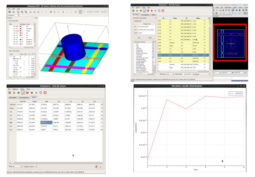
Q: What is the topology of an FPD array?
The structure of the FPD is composed of light-emitting pixel units arranged in a two-dimensional array. As shown below, the cell is the pixel unit. There are three sub-pixels in the cell: red (R), green (G), and blue (B). From the circuit level, the FPD is the top-level circuit, and the cell is the sub-circuit of the next level, and the sub-pixel circuit is the sub-circuit of the next level.
Hierarchical structure of FPD circuit
Each cell has the same circuit structure, and each sub-pixel circuit in the cell also has the same circuit structure. These cells have the same circuit structure, and their states are also similar when working, so we can define the cell as a basic unit. The circuit parts with the same structure and the same state only need to store and simulate only one basic unit, and the simulation data is shared with other units, which greatly reduces the simulation time and the required memory.
In addition, using the heterogeneous computing structure of CPU+GPU is a new direction to improve the speed of full-scale circuit simulation 6, 7.
Q: What is your approach for RC extraction to get parasitics into a more accurate netlist for simulation?
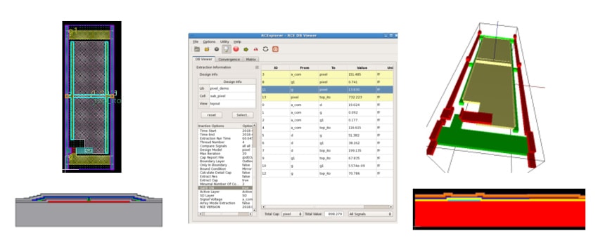
EMPYREAN’s parasitic RC extraction tool RCExplorer FPD provides pixel and touch panel capacitance and resistance simulation analysis tools for a variety of FPD design application scenarios. Based on the parasitic capacitance resistance extraction technology of the accurate three-dimensional field solver, the adaptive meshing technology is adopted to accurately simulate the coupling capacitance.
The 3D field solver is based on electric field analysis and uses numerical calculation methods to solve the Laplace equation. The problem of solving capacitance can be transformed into solving the induced charge of a conductor under a certain bias voltage. This problem can be solved by solving the following electromagnetic field equations 8.
The RCExplorer FPD tool also supports pixel-level liquid crystal capacitance extraction, as shown next. At the same time, it can support Gate-on capacitor extraction.
Pixel liquid crystal capacitance extraction
Q: Can you extract a touch panel design layout?
Yes, the RCExplorer FPD can simulate the capacitance of the touch panel in the touch panel design. Due to the large size of the touch panel design and the high requirement for capacitance accuracy, it’s challenging to ensure both high accuracy and performance requirements. The tool uses a meshing method based on following advanced technologies, such as, a mixture of triangle elements and trapezoid elements; intelligent meshing engine automatically determines the degree of density; efficient and adaptive mesh encryption 9, 10; multithreading and multitasking parallel calculations, etc., to ensure the calculation accuracy and calculation speed to meet the design requirements. At the same time, the tool also supports Floating Signal and Finger settings.
With the parasitic capacitance and resistance extracted by RCExplorerFPD, users can perform post-layout analysis to check whether the design load is within an acceptable range, and help designers optimize the layout load design.
Touch Panel RC Extraction
Q: How are the thermal-electrical characteristics analyzed for FPD arrays?
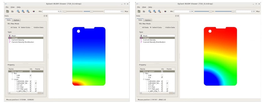
High-precision OLED device current control is extremely important to the uniformity of OLED FPD light emission, and so it is critical to ensure the stability of power and ground potential 11. The EMPYREAN Artemis FPD high-resolution full-panel layout thermoelectric analysis tool analyzes the power/ground voltage drop distribution, current density distribution, and temperature distribution of the FPD, which can effectively help designers optimize the design.
This tool adopts advanced techniques such as accurate resistance calculation method, cascade array netlist output, hierarchical fast calculation method, heat conduction and heat convection, etc., which can quickly and accurately perform full-panel analysis.
The tool uses an array-based accurate resistance calculation acceleration method. The entire flow uses a two-dimensional field solver to calculate the highest precision resistance network, and uses the pixel array hierarchy to quickly calculate the voltage and current distribution of the overall resistance network. It calculates the power and ground potential of each TFT.
FPD voltage distribution analysis
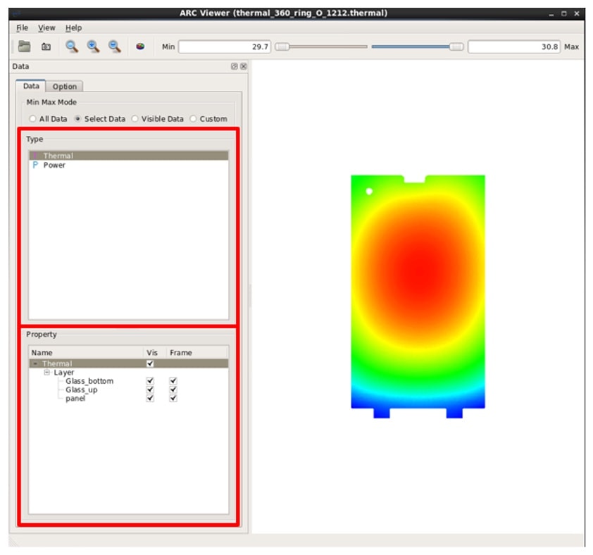
With the wire resistance between the nodes of the resistive network and the voltage across the nodes, together with the device voltage and current information, we can calculate the power value at each node of the entire panel.
With the power distribution, according to the mixed model of heat conduction and heat convection, we can get the heat distribution of the panel.
FPD temperature distribution analysis
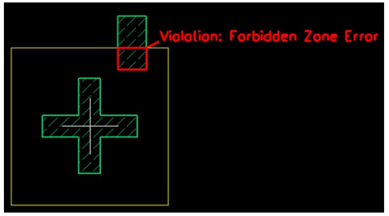
Q: Why is it important to have Mark Rule Checks (MRC)?
MRC inspection is an important part of the design flow after the mask layout is completed. EMPYREAN’s MRC tool provides the Mask and Glass design engineers with tools to check the correctness of Mark placement. Mark is an important reference for process alignment of exposure, etching and other machines, and has zero tolerance for errors. The MRC tool provides an automated Mark inspection method to improve the reliability of Mark design. It can check more than ten rules and their combinations, such as forbidden zone, symmetry, standard Mark position comparison, and provide clear and easy-to-understand annotation cartoons to mark the location of errors, such as forbidden zone inspection errors.
MRC forbidden zone inspection
Q: What are challenges of the largest panel masks?
The Split Panel function provides an FPD design engineer with the function of cutting the panel layout into multiple mask layouts. Split Panel is an essential function in large-size stitching design. When the size of the Panel exceeds the size of the exposure machine, one exposure cannot complete the production of a large-size panel, and it is necessary to stitch the design for multiple exposures to finally complete the production of a panel. Based on the layout of the large-size panel and the size of mask, the Split Panel cuts the panel through guideline or cartoon direct cutting method, thereby dividing it into multiple mask layouts.
Schematic diagram of Split Panel
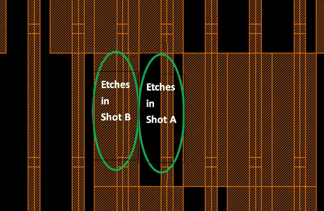
The Split Panel function can automatically call the Mosaic function. If the boundary between two adjacent exposures is a straight cut, the human eye can clearly distinguish the exposure dividing line in the light-emitting area of the panel, because the human eye is more sensitive to the shape of the long strip.
In order to circumvent the above problems, it is necessary to perform fuzzy cutting at the exposure boundary. The method is to randomly select pixels for photolithography within the range parallel to the division line on both sides of the abstract exposure division line in the light-emitting area (AA) . For example, for a certain layer, if a certain pixel is to be exposed in shot A, its layer graphics will be kept in shot A cell. On the contrary, use a rectangle of the same size as the pixel outline to completely cover it. The goal is to make the dividing line non-linear and irregular, avoiding the problem that the human eye can recognize regular boundary. The function of randomly dividing pixels into two or more shot cells is called a Mosaic function.
Mosaic function in Split Panel
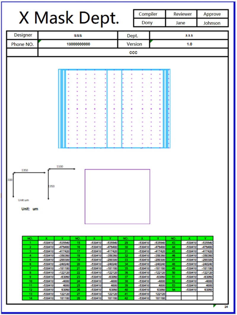
Q: What does the production department receive from the FPD design group?
After both the Mask and Glass layouts are completed, the Mark information needs to be extracted to the production department. At this time, the Job File function is required. The Job File function automatically extracts the coordinate list of the specified marks and outputs the process file according to the specified template or rules for the post-layout steps. Generally speaking, the output process file will be used as the reference coordinate file for machine work and other production processes.
Job File data
Summary
In the three blog series we’ve covered a lot of details on how modern FPD designs can be automated through the successive steps of: circuit schematic, layout, SPICE device modeling, SPICE circuit simulation, RC layout extraction, IR-drop analysis, thermal analysis, design verification and mask analysis.
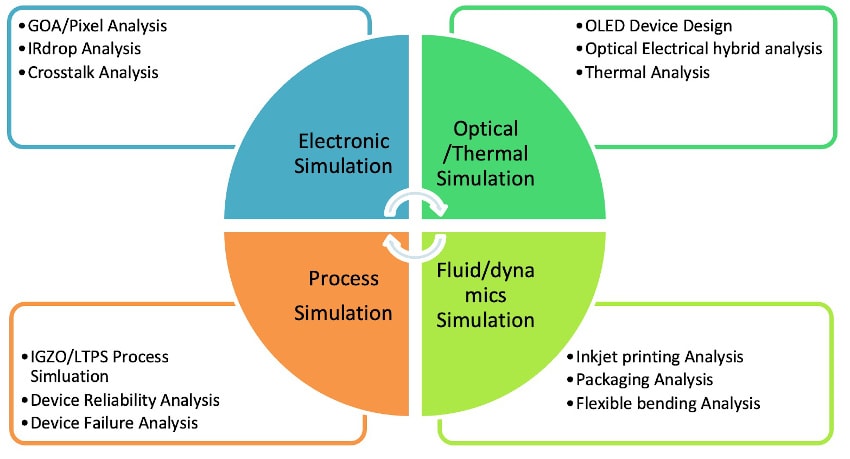
Empyrean has been focusing on the FPD design automation area since 2012, so give them a call when your team ventures into this product development area. Expect new developments from Empyrean in the area of design kits for OLED and Micro LED devices, and improved optoelectronic hybrid simulation. Going beyond electrical simulation of FPD, there are many areas for expansion.
Empyrean FPD technology outlook
References
Carl Ebeling. “Gemini II: A Second Generation Layout Validation Tool”,Proceedings of the IEEE International Conference on Computer Aided Design (ICCAD-88), pp. 322-325, November 1988
Zhou Peide, “Computational Geometry: Algorithm Design and Analysis”, Tsinghua University Press, 2005
Thomas H. Cormen, Charles E. Leiserson, “Introduction to Algorithms”, China Machine Press, 2006
Liu Weiping, Zhou Zhenya, Cai Yici, “A Hybrid Acceleration Algorithm for Post-layout Parallel Circuit Simulation”, Journal of Computer-Aided Design and Graphics Theory, 28(11),2016-2020, 2016
Yang Liu, “A new generation high performance parallel circuit simulation tool”, China Integrated Circuit, October 2016
Lifeng Wu, “Enable Full Panel Circuit Simulation to Improve Brightness Uniformity”, Invited Paper, 9th International Conference on CADTFT, ShenZhen, China, November, 2018
Lifeng Wu, “Exploring New Tides of EDA”, Invited Paper, 25th Asia and South Pacific Design Automation Conference (ASPDAC), Beijing, China, January 2020
Lu, T., Wang, Z., and Yu, W. “Hierarchical Block Boundary-Element Method (HBBEM): A Fast Field Solver for 3-D Capacitance Extraction.” Microwave Theory & Techniques IEEE Transactions on 52.1:10-19.
Lu Taotao, Wang Guanghui, Hou Jinsong, Wang Zeyi, “Hierarchical h-Adaptive Computation in VLSI 3-D Capacitance Extraction”, Chinese Journal of Semiconductors, 543-549,2002
Jinsong Hou,Zeyi Wang,Xianlong Hong,“The hierarchical h-adaptive 3-D boundary element computation of VLSI interconnect capacitance”,ASPDAC,1999
J. Sun, “IR-drop compensation for large size AMOLED”, IDW Tech. Dig., pp. 183-184, December 2011
Probably the least appreciated and most critical thing I spend my time on when driving custom silicon projects is setting up the entire framework to get everyone talking and in rhythm with each other. Only supplier selection is more critical to the project’s success than this.
All system custom silicon projects where the silicon is not designed and manufactured in-house by the system company require at least two companies to directly interface with each other: the system company and the silicon supplier company. Each one of these two companies has other companies they subcontract work to. These become critical to the custom silicon development process at some stage of the project.
System company teams
Typically, the system company works with a contract manufacturer (CM), and that CM interacts with the silicon supplier whenever there is an FA from the build. The CM sends units back for analysis at the silicon supplier’s lab. The CM also needs to discuss with the silicon supplier the types of reels to be used for shipments, part markings, and eventually the CM will be submitting POs for the MP ramp.
The system company has many cross functional teams. Any or all of these teams could be involved in the integration of this component into the system: software, firmware, security, EE, ME, system reliability, component engineering, PCB design, thermal team, signal integrity, silicon management, system project management, sub-system teams and their project management, battery team, antenna/RF team, test fixture team, GSM, and/or legal.
Silicon supplier company teams
In parallel, the silicon supplier interacts with a package and test contractor, and a foundry for wafer manufacturing. The silicon supplier could also be subcontracting external design houses, quality testing labs, failure analysis labs, etc… Some silicon suppliers have in-house foundries, and package and test in-house, but most do not. The system company generally will not interact with the foundry or the package and test subcontractor EXCEPT if they are interested in aggregating their volumes to get better pricing and terms. So for example, a system company may be buying many different chips from different silicon suppliers, but most are using the same foundry or the same packaging houses. They may decide to go directly and tell those foundries to aggregate their total volumes when quoting wafer or package prices to the silicon supplier for the parts for which they are the end customer. In this way, the system company obtains a price reduction.
The silicon supplier company has some core teams which at some point will be interacting with the system company. These are: design (analog and digital) team, validation/apps team, test team, layout team, verification (AMS, DV and analog) team, package, sales and marketing teams, FAEs, and software/firmware teams.
If there are not already enough teams, people and companies involved, add to the mix that typically the system company, the silicon supplier and their subcontracted parties are in different countries/regions.
Here are some basic things that need to be implemented to manage this complexity of human and technical challenges:
Communication.
You will need to implement multiple regular interactions to keep people aligned and informed. The main meetings that need to be programmed are: regular sync call between the system and silicon supplier teams, internal cross functional sync meeting at the system company, in person design reviews and in person vendor selection reviews, meetings to obtain phase sign off from executives for all phases, and many other contact points as needed to deep dive on items. Make sure to establish a ticket system to track actions throughout the entire process . You will need to document a lot, and share between different sides as needed. CustomSilicon.com offers some packages that manage some or all of these interactions.
Ensure to have a process to manage the system custom silicon engagement.
CustomSilicon.com implements a process, and manages both the system and silicon companies such that there is a really strong connection between all teams, the deliverables are clearly communicated, and the development phases are signed off by all stakeholders such that there is cross functional and multi company alignment at every stage of the project. The process should be captured in the contracts, and the sign offs should be used as triggers. This is not legal advice, and I am not lawyer, so please ensure to seek legal counsel to draft good contracts. The silicon manager will drive the sign offs with the system company, and also drive to closure all issues with the silicon supplier such that at the end of a phase a concise precise escalation can be presented to the system company executives for their approval.
Establish a clear stakeholders list, establish what authority each of them has, and for what aspect of the project.
One of the least appreciated, and most critical aspects of driving cross functional teams is that it is imperative that no one usurps someone else’s rightful authority over the domain for which they are responsible. One very pernicious human factor that destroys effective collaboration is the practice of calling “working meetings” or “executive update meetings” with decision makers to push a one sided agenda. The people that call the meeting leave out other stakeholders who hold some contrary views. A healthy debate over the proposals is prevented. Then an attempt is made to gain approval from the decision makers without presenting all facts and views. This type of political maneuver will seriously derail cross functional team collaboration. It will also destroy trust and goodwill in the program. The silicon manager MUST not let this happen by ensuring everyone that is a rightful stakeholder is signed off for each phase and included in discussions directly relevant to their domains. The other issue that needs to be addressed is not allowing people who are NOT rightful stakeholders to impede or block progress from occurring. Sometimes they demand to be included in meetings to which they have no agenda items to cover. They may also want to “vote” on decisions to which they are not rightful stakeholders. Sometimes it is ok to allow non-stakeholders to sit in meetings. But in my experience this can backfire as you then start seeing how these political maneuvers have some malicious intent which later becomes clear. The silicon manager then has to deal with the blowback to keep the program on track. So to keep the peace and sanity, it is very important that everyone that is a stakeholder is accounted for and included, and everyone that isn’t is scrutinized if they insist on being involved without a clear logical explanation.
There are many difficulties in driving a custom silicon project that only common sense, people management, determination, technical competency in the systems and silicon domains, and a solid process can overcome so that you can go from concept to mass production with confidence. I hope this short list above is a helpful first step for you.
CustomSilicon.comis the leading consulting firm in the custom silicon strategy and project management space for AR/VR, automotive, mobile, server, crypto, sensors, security, medical, space and more.
Raul has 20 years of combined experience in the system electronics and silicon industries. He is currently responsible for major system company’s custom silicon and sensor projects with projects approaching 30 total chips. Raul was the directly responsible silicon manager for 18 chips ramped to mass production at Apple for iPhone and iPad, and 23 total chips ramped to mass production counting projects where he was an expert reviewer. Raul was directly responsible for the development of mobile processor System PMICs for the iPad2, New iPad, iPad mini, iPad 4 and iPhone 5s. Other silicon included, backlight/display power for iPhone 5 and iPhone 5s, lightning connector silicon and video buffers. He managed supplier teams across the Globe.
Our network of experts provide our clients with an A+ silicon management team from day one.
System-level expertise, once the domain a few architecture specialists, is now shouldering its way everywhere into chip design and verification. In virtual modeling together with OS and application software certainly. That now couples into mixed-level system-verification, using different levels of abstraction for different parts of the system. In architecture analysis for major components, connecting to frameworks especially for AI. For hardware and software partitioning and experimenting with memory architectures. Verifying your architectural model against extensive test suites. And finally synthesizing the design to RTL while experimenting with further micro-architectural performance and power choices. You need more ESL expertise for non-experts.
When ESL becomes essential but is not a core-expertise
At one time ESL was dismissed as a fringe concept, interesting primarily to academics and super-early adopters. However, AI and the sheer size of AI test databases has put that idea to rest. If you want to do more than simply drop your trained DNN on an AI accelerator, especially if you want to experiment with memory optimization, you’re going to have to go through some kind of ESL path. If you want to verify image recognition test suites on the design, you have to do that in ESL. Attempting this at RTL would be insanely slow. And if you have to be competitive in performance and power, you have to optimize at the micro-architectural level. Fiddling with clock gating isn’t going to get you there.
The challenge for many of us is that while we have teams of smart people, they’re expert in RTL, not ESL. Now they have to learn about TensorFlow, PyTorch and other strange frameworks. And they have to learn about ESL. They’re smart, they’ll get there but is there any way you can speed up that learning curve? That’s the goal of CircuitSutra. They’re a consulting organization providing assistance in accelerating adoption of ESL methodologies for active design teams.
Endorsements
They’ve already proven their worth in projects at LG, TI and GreenSocs, among others. One endorsement was for the company developing the TLM Kit and sockets for a proprietary SoC bus. The kit they built is compliant with Accellera TLM2.0 and was used to develop the SystemC models of peripheral IP. Even better, the kit relieves the model developer from the complexity of TLM rules for modeling data communication at different abstraction levels. These range from loosely timed to cycle accurate TLM, with very simple-to-use abstraction-independent APIs. The level of abstraction can be changed at run time, allowing the modeler to dynamically adjust the performance accuracy trade-off, for instance, to support “fast-forwarding”. CircuitSutra came up with an innovative design that is extensible and can be easily adapted for any SoC bus architecture. They also developed a very comprehensive test-suite and ensured high functional coverage.
Another mentioned that CircuitSutra have successfully executed several modeling projects for their SoC bus architecture, Virtual Platform development, Integrating Virtual platform with the debugger and other tools, OS bring up on the virtual platform, SystemC Models of Image processing IP, Audio IP and OS bringup on VP. They particularly called out CircuitSutra as having strong expertise in modeling domain.
Also, very topical, they’ve added ESL expertise around RISC-V. Sounds like a company you should get to know.
You can learn more about the company in this video. And you can learn more about CircuitSutra HERE.
It should come as no surprise that S2C would step out in front with a high-density FPGA prototyping hardware platform for users who would like to scale to large numbers of FPGAs and high performance. That’s exactly what they have done with their new Prodigy Logic Matrix family of FPGA prototyping products that S2C announced in December. S2C has been in the FPGA prototyping business now for over almost two decades and has been a leader in high-quality hardware and complete solutions FPGA prototyping. Other large EDA suppliers have FPGA prototyping systems that support large numbers of FPGAs, but they’re encumbered by the supplier’s own ideas about optimal FPGA connectivity and compatibility with their other proprietary EDA tools such as emulation – often with a cost of lower prototyping performance. S2C’s new Logic Matrix family is architected for maximum flexibility without presumptions about FPGA interconnect or design flow – just an unencumbering assumption that the user may have their own innovative ideas about optimal FPGA interconnect to achieve the highest prototyping performance and utility.
Prodigy Logic Matrix
Each Logic Matrix comes with 8 FPGAs and is easily mounted in a 42U server rack – and up to 8 Logic Matrix may be loaded into a single standard server rack supporting up to 64 FPGAs per rack. Scaling to even more FPGAs may be accomplished by connecting multiple server racks – a project for seasoned FPGA prototyping veterans with a vision for prototyping multi-billion gate chip designs. The Logic Matrix LX1 is available now and sports the relatively mature Xilinx Virtex UltraScale VU440 FPGAs with an estimated prototyping capacity of 240 million usable ASIC gates. The Logic Matrix LX2 will follow in Q2 of 2021 and will use the newer Xilinx UltraScale+ VU19P, upping the estimated prototyping capacity to 392 million usable ASIC gates.
The Logic Matrix board format is open with plenty of connectors for all levels of interconnect – FPGA to FPGA on each Logic Matrix, Logic Matrix to Logic Matrix within a server rack, and rack to rack connections. The 8 FPGAs are surrounded by high-pin count Samtec connectors for single ended I/O or LVDS pairs (64 connectors), high-performance Samtec connectors (8 connectors), and mini-SAS connectors (80 connectors).
Sc2 EDA Logix MatrixS2C also made mention in the Logic Matrix family announcement of two other pieces of their high-density prototyping solution that are “soon to be released” – RTL partitioning and what S2C calls hierarchical connectivity to address local, Logic Matrix-to-Logic Matrix and rack-to-rack interconnect.
S2C’s other prototyping productivity tools may be paired with the Logic Matrix, including ProtoBridge and the MDM Debug Module. ProtoBridge is a PCIe to AXI interface between the FPGA prototype and a host PC for stimulating the prototype with high-speed (1GB/s) software-modeled transactions, video streams, or other streams of stimulus.
MDM is S2C’s multi-FPGA Debug Module that offers multi-FPGA signal viewing in a single viewing window. MDM comes with external hardware that provides 8GB of trace waveform storage without consuming user memory.
To round out S2C’s complete prototyping solutions with Logic Matrix, S2C offers a rich library of what it calls Prototype Ready IP – Daughter Cards that plug-and-play with the Logic Matrix to speed the creation of the prototyping environment around the FPGA prototype.
S2C is a worldwide leader of FPGA prototyping solutions for today’s innovative designs. S2C was founded in 2003 by a group of Silicon Valley veterans with extensive knowledge in ASIC emulation, FPGA prototyping, and SoC validation technologies. The Company has been successfully delivering rapid SoC prototyping solutions since its inception. S2C provides:
Rapid FPGA-based prototyping hardware and automation software
Prototype Ready™ IP, interfaces and platforms
System-level design verification and acceleration tools
With over 400 customers and more than 2000 systems installed, S2C’s focus is on SoC/ASIC development to reduce the SoC design cycle. Its highly qualified engineering team and customer-centric sales force understands our users’ SoC development needs. S2C systems have been deployed by leaders in consumer electronics, communications, computing, image processing, data storage, research, defense, education, automotive, medical, design services, and silicon IP. S2C has offices and distributors around the globe including the US, UK, Israel, China, Taiwan, Korea and Japan.
Back in April, I posted a blog about SmartDV, The Quiet Giant in Verification IP and More. This is a story about the “more” part of that statement. Acquisition activity in the semiconductor sector has been quite brisk this year. A bright spot in what could otherwise be a sometimes-overwhelming series of bad news. Acquisition has been a focus at SmartDV as well. The company recently announced the acquisition of a new line of design IP controllers for high-speed communications. Here is a bit more color on that announcement and how SmartDV expands its design IP portfolio with an acquisition.
What Was Announced
The announcement centers on the acquisition of a design IP business and products from a leading, pure-play engineering services company. The identity of the company and the price tag of the acquisition were not disclosed. Independent of those items, there is a lot to the story that highlights the strength and significance of this acquisition. A key piece of information is that the IP portfolio is silicon-proven and includes minimal area controller IP for popular standards including mobile and mobile-Influenced (MIPI) and universal serial bus (USB) interfaces.
The Importance of Silicon Validation
Silicon validation of standards-based IP like this is a critical item to reduce risk and time-to-market. Since the IP is coming from an engineering services company, silicon validation will be a key benefit. The release reports all the IP titles are implemented in numerous chip design projects and a variety of consumer electronics devices. Having worked at a company that offered IP and ASICs (eSilicon), I can tell you this is key differentiator. At eSilicon, we didn’t just design IP blocks and do one test chip for characterization before offering it for sale. Instead, we would use these IP titles in our ASIC business on real production chips. The validation from this kind of activity is quite a bit more robust than a characterization test chip alone.
Deepak Kumar Tala, SmartDV’s managing director commented on the fit of the IP portfolio and its source. “The acquisition of a Design IP portfolio strengthens our offerings for mobile and high-speed communications application markets. The purchase comes from a company noted for exceptional customer support and service. With this reputation, its high-quality, highly configurable and silicon-proven Design IP is a good fit for SmartDV’s standards.”
The Details
The portfolio is quite extensive and includes:
MIPI
MIPI camera serial interface (CSI-2) transmitter and receiver controller design IP for C-PHY and D-PHY
MIPI display serial interface (DSI) and DSI-2 transmitter and receiver design IP for C-PHY and D-PHY
MIPI CSI-3 host and device design IP
Universal flash storage (UFS) interface 2.1 and 3.0 host and device design IP
MIPI unified protocol (UNIPRO) controller 1.6 and 1.8 design IP
I3C interface master and slave controller design IP
USB
Silicon-proven and USB-Implementers Forum (USB-IF) certified
USB 1.1/2.0 device controller
x 5G device controller
x 5G host controller
x 5G hub controller
x 5G dual-role controller
USB-IF certified
x 10G device controller
Verified and FPGA validated
USB On-The-Go (OTG)
USB SuperSpeed Inter-Chip (SSIC)
0 xHCI host controller
Design Ready
0 device router
Availability and To Learn More
Licenses for the new IP include validation platforms along with firmware support to functionally validate chip design prior to tape out and mitigate risk. All controller design IP is pre-verified and delivered as a comprehensive solution, complete with a verification suite, clock domain crossing, synthesis and logic equivalence checking constraints and waivers, as applicable. They are reusable at the system-on-chip (SoC) level and proven interoperable with partner PHY solutions. I can tell you from first-hand experience interoperability between the controller and PHY is really important, this is a key benefit.
The new portfolio is available now and backed by an experienced team. Pricing is available upon request. You can email requests for data sheets or more information to sales@Smart-DV.com. The news is true, SmartDV expands its design IP portfolio with an acquisition.
Quantum teleportation is a technique for transferring quantum information from a sender at one location to a receiver some distance away. While teleportation is portrayed in science fiction as a means to transfer physical objects from one location to the next, quantum teleportation only transfers quantum information. [1]
For the first time, a team of scientists and researchers have achieved sustained, high-fidelity ‘quantum teleportation’ — the instant transfer of ‘qubits’ (quantum bits) the basic unit of quantum information. the collaborative team, which includes NASA’s jet propulsion laboratory, successfully demonstrated sustained, long-distance teleportation of qubits of photons (quanta of light) with fidelity greater than 90%. the qubits were teleported 44 kilometers (27 miles) over a fiber-optic network using state-of-the-art single-photon detectors and off-the-shelf equipment.[5]
Important point to keep in mind is quantum teleportation is the transfer of quantum states from one location to another using quantum entanglement, where the two particles in separate locations are connected by an invisible force, famously referred to as “spooky action at a distance” by Albert Einstein. Regardless of the distance, the encoded information shared by the “entangled” pair of particles can be passed between them. An interesting note is that the sender knows neither the location of the recipient nor the quantum state that will be transferred.
By sharing these quantum qubits, the basic units of quantum computing, researchers are hoping to create networks of quantum computers that can share information at blazing-fast speeds. But keeping this information flow stable over long distances has proven extremely difficult due to changes in the environment including noise. Researchers are now hoping to scale up such a system, using both entanglement to send information and quantum memory to store it as well. [5]
On the same front, scientists have advanced their quantum technology research with the development of a chip that could be scaled up and used to build the quantum simulator of the future using nanochip that allows them to produce enough stable photons encoded with quantum information to scale up the technology. The chip, which is said to be less than one-tenth of the thickness of a human hair, may enable the scientists to achieve ‘quantum supremacy’ – where a quantum device can solve a given computational task faster than the world’s most powerful supercomputer. [6]
Quantum Entanglement
In quantum entanglement particles that have interacted at some point retain a type of connection and can be entangled with each other in pairs, in a process known as correlation. Knowing the spin state of one entangled particle – up or down – allows one to know that the spin of its mate is in the opposite direction. Quantum entanglement allows qubits that are separated by incredible distances to interact with each other instantaneously (not limited to the speed of light). No matter how great the distance between the correlated particles, they will remain entangled as long as they are isolated. [2]
Quantum Teleportation: Paving the Way for a Quantum Internet
In July, the US Department of Energy unveiled a blueprint for the first quantum internet, connecting several of its National Laboratories across the country. A quantum internet would be able to transmit large volumes of data across immense distances at a rate that exceeds the speed of light. You can imagine all the applications that can benefit from such speed.
Traditional computer data is coded in either zeros or ones. Quantum information is superimposed in both zeros and ones simultaneously. Academics, researchers and IT professionals will need to create devices for the infrastructure of quantum internet including: quantum routers, quantum repeaters, quantum gateways, quantum hubs, and other quantum tools. A whole new industry will be born based on the idea of quantum internet exists in parallel to the current ecosystem of companies we have in regular internet.
The “traditional internet “, as the regular internet is sometimes called, will still exist. It is expected that large organizations will rely on the quantum internet to safeguard data, but that individual consumers will continue to use the classical internet.
Experts predict that the financial sector will benefit from the quantum internet when it comes to securing online transactions. The healthcare sectors and the public sectors are also expected to see benefits. In addition to providing a faster, safer internet experience, quantum computing will better position organizations to solve complex problems, like supply chain management. Furthermore, it will expedite the exchange of vast amounts of data, and carrying out large-scale sensing experiments in astronomy, materials discovery and life sciences. [2]
The device roadmap for the next few advanced process nodes seems relatively clear. The FinFET topology will subsequently be displaced by a “gate-all-around” device, typically using multiple stacked channels with a metal gate completely surrounding the “nanosheets”. Whereas the fin demonstrates improved gate-to-channel electrostatics due to the gate traversal over the height and thickness of the fin, the stacked nanosheets have further improved this electrostatic control – subthreshold leakage currents are optimized.
An extension to the nanosheet topology that has been proposed is the “forksheet”, as depicted in the figure below. [3]
The goal of the forksheet R&D is to eliminate the nFET-to-pFET device spacing rule (for a common gate input connection), isolating the two sets of nanosheets with a thin oxide. The tradeoff for this attractive gain in transistor density is that the gate again surrounds the channel volume on three sides – “FinFETs turned on their sides” is a common forksheet analogy.
Although the dates for high-volume manufacturing (HVM) of post-FinFET nodes are somewhat fluid, it is expected that these evolutionary nanosheet/forksheet device topologies would emerge in the 2024-25 timeframe.
There is active process development and device research underway for a myriad of alternatives to the nanosheet. Assuming that the “nano” device topology will be used for at least a couple of process nodes, research needs to be aggressively undertaken now, if any new device is to reach HVM in 2028-30.
At the recent IEDM conference, Synopsys presented their forecast and design-technology co-optimization (DTCO) evaluation results for one of the leading device alternatives for the “1nm” node in this timeframe. [1] This article summarizes the highlights of their presentation.
The “1nm” Node
The figure below depicts the straight-line trend of transistor density across several recent process nodes. (This graph was provided as part of collaboration between Synopsys and IC Knowledge, Inc.)
Several things to note about this graph:
the node names on the X-axis represent a simple transition from the 14nm node, with each successive data point defined by the Moore’s Law linear multiplier of 0.7X
Frequent SemiWiki readers are no doubt aware that the actual nomenclature assigned by a foundry to successive nodes has received some “marketing input”. For the sake of this discussion, using the 0.7X names is appropriate, if the goal of the DTCO process development is indeed to remain on this curve.
the density data points at each node represent metrics from multiple foundries
the data points include separate measures for logic and SRAM implementations
Logic density is typically associated with the foundation library cell implementation commonly used with the foundry technology. For example, the area of a 2-input NAND cell reflects 4 devices in the cell using:
the contacted poly pitch (CPP)
the number of horizontal metal tracks in the cell (for signals and supplies)
the cell adjacency isolation spacing (“diffusion breaks” versus tied off dummy gates between cells)
Another key cell dimension is the area of a (scannable) data flip-flop. The transistor density calculation above uses a logic mix of NAND and FF cells for each logic data point.
Of particular note is the assumption for the device topology used in the Synopsys projections for the 1nm node. Active research is underway to evaluate several non-silicon field-effect device types in a timeframe consistent with this node – e.g., 2D semiconducting materials (MoS2) and 1D carbon nanotubes. For the goal of staying on the transistor density curve, the Synopsys TCAD team pursued DTCO process definition for a 3D “Complementary FET” (CFET) implementation. The figure below illustrates the CFET cross-section.
An attractive feature of the CFET technology is the similarity to the nanosheet topology, which will have years of manufacturing experience in the 1nm node timeframe. The novelty of the CFET approach is the vertical positioning of pFET and nFET nanosheets.
The CFET topology leverages the typical CMOS logic application where a common input signal is applied to the gate of both an nFET and pFET device. (The unique case of a 6T SRAM bitcell with nFET-only word line pass-gates will be discussed shortly.)
The figure above illustrates how the pFET nanosheet resides directly below the nFET nanosheet(s). In the figure, two nFET nanosheets are present, narrower than the pFET – as space is required to contact the pFET source and drain nodes, the nFETs are reduced in width. The two nFETs in parallel will provide comparable drive strength to the pFET. (SRAM bitcell design in CFETs utilizes a different strategy.) An M0 contact over active gate (COAG) topology is also shown extending this recent process enhancement.
The processing of CFET devices requires specific attention to the sequential pFET and nFET formation. Epitaxial growth of SiGe for the pFET source/drain nodes is used to introduce compressive strain in the channel for improved hole mobility. pFET gate oxide and metal gate deposition are then performed. The subsequent epitaxial Si growth for nFET source/drain nodes, followed by gate oxide and metal gate deposition, must adhere to materials chemistry constraints imposed by the existing pFET device.
Buried Power Rails
Note the assumption for the 1nm node that the local VDD and GND distribution will be provided by “buried power rails” (BPR), resident below the nanosheets in the substrate. As a result, both “shallow” (device) and “deep” (BPR) vias are required. The metal composition of the BPRs and the vias is thus a critical process optimization to reduce the parasitic contact resistance. The (primary) metal needs to have low resistivity and be deposited with extremely thin barrier and liner materials in the trench.
Speaking of parasitic, the (simplified) layout diagram below highlights a unique advantage of the CFET topology. [2]
The three-dimensional orientation of the CFET devices eliminates the gate traversal between separate nFET and pFET regions. Also, in comparison to a FinFET device layout, the parallel run length of the gate-to-source/drain local metallization is significantly reduced. (The small gate length extension past the nanosheet is shown in the figure.) As a result, the device parasitic Rgate resistance and Cgs/Cgd capacitances are vastly improved with the CFET.
CFET SRAM Design
The implementation of a 6T SRAM bitcell in a CFET process introduces several tradeoffs. The Synopsys DTCO team opted for unique design characteristics, as illustrated below.
an nFET pulldown : pFET pullup ratio of 2:1 is readily achieved
The two smaller nFET nanosheets shown earlier for a 1:1 logic drive strength ratio are the same width as the pFET in the SRAM bitcell, giving the 2:1 drive strength. (Note that this would be comparable to a FinFET bitcell, where the number of nFET fins is 2 and the number of pFET fins is 1.)
a modified pair of nFET pass gate devices is implemented
The two nFET nanosheets used for the pass gates are (slightly) weaker than the pull downs; the gate is only present over three sides of the nanosheet. This “tri-gate” configuration provides for a denser bitcell, and optimizes the relative strengths of the pass gate:pull down nFET devices for robust cell read margins.
the pFET nanosheet under the pass gate devices now becomes an inactive “dummy” gate
a unique “cross-couple” layer (at the level of the M0 vias) is used for the internal 6T cell interconnections
DTCO analysis early in process development utilizes TCAD simulation tools, to represent materials litho patterning, materials deposition, and (selective) etching profiles. This early optimization work provides insights into the required process windows, as well as the expected materials dimensions and electrical properties, including channel strain to optimize free carrier mobility.
Subsequent parasitic extraction, merged with the device models, enables preliminary power/performance measures for the new process, combined with the device layout area for a full PPA assessment. The (rather busy) figure below provides a visualization of the DTCO analysis for the SRAM bitcell described above.
Summary
At IEDM, the Synopsys TCAD team provided a peek into the characteristics of the “1nm” node, based on a CFET device topology, with one pFET nanosheet below two nFET nanosheets. Buried power rails were also assumed. The lithographic assumptions were based on the utilization of (high numerical aperture) EUV – e.g., a 39nm CPP (with COAG) and a 19nm M0 metal pitch. A unique SRAM bitcell design approach was applied, both for the relative PU:PD:PG drive strengths and for an internal cross-couple interconnect layer.
The results of this DTCO analysis suggest that the 1nm CFET node may indeed be able to maintain an aggressive transistor density, approaching 10**9 transistors/mm**2. It will be extremely interesting to see how this forecast evolves.
I would encourage you to look at this IEDM presentation.
-chipguy
References
[1] Moroz, V., et al, “DTCO Launches Moore’s Law Over the Feature Scaling Wall”, IEDM 2020, paper 41.1.
[2] Ryckaert, J., et al, “The Complementary FET (CFET) for CMOS scaling beyond N3”, VLSI Technology Symposium 2018, p. 141-142.
[3] Collaert, Nadine, “Future Scaling: Where Systems and Technology Meet”, ISSCC 2020, Paper 1.3.
The Automotive News had a standout year in 2020 – thriving at a time when many publishers suffered. With factories and dealerships shuttered in the spring due to the pandemic, the outlook was bleak but the Automotive News dug in amplifying its reporting with multiple podcasts and video content documenting the ups and downs of the industry recovery.
Nowhere was this community service and news amplification more focused than in the Daily Drive podcast where Automotive News Publisher Jason Stein and fellow editors and reporters recorded interviews with industry notables describing their day-to-day experiences and pandemic responses. Paired with the Shift Automotive podcasts, Automotive News pumped out hundreds of these enlightening segments – all freely accessible for listeners stuck at home or needing background noise for a socially distanced workout.
The best of these podcasts, bar none, was Jason Stein’s exclusive interview with Tesla Motors’ CEO Elon Musk. And the moment that crystalizes the events of 2020 and Tesla’s and Musk’s role in the industry comes at 8:20 of the latest condensation of that interview where Stein asks Musk if Tesla did any customer research when designing its upcoming Cybertruck.
The moment comes as Musk, predictably, responds that, of course, Tesla didn’t do any customer research:
“Oh, zero. Customer research. Ha ha ha ha ha. No. I mean. I mean, we just made a car that we thought was awesome. You know, it looks super weird. I just wanted to make a futuristic, like a futuristic battle tank. Something that looked like it could come out of ‘Blade Runner’ or ‘Aliens’ or something like that – you know – but that was also highly functional, had incredible capabilities, faster than a Porsche 911 and more towing power, more truck capability than a Ford F-150.”
It’s difficult to render in print, but Musk’s laugh in the segment is positively diabolical. One hears the villainous cackle of every over-confident, ghoulish baddie from every Batman, Marvel Comics, or 007 movie ever made, combined. Stein follows up his question by asking Musk to assess his own management style and gets what sounds like an almost too-perfect response from Musk: “I must be doing something right.”
And who’s to argue with that? In a separate section of the interview Musk notes his market cap exceeds the combined value of the rest of the entire automotive industry. Again, Musk takes the stance of stating a simple fact without need of exaggeration.
This week commenced with Tesla’s stock having its debut in the S&P 500 where it waffled a bit before finding its groove and settling in. As 2021 approaches, storm clouds loom as lucrative carbon credits disappear with the pending PSA-FCA merger expected to be finalized at the end of January 2021.
As InsideEVs reports, it was those carbon credits that allowed Tesla to show five consecutive quarters of profit cementing its candidacy for S&P 500 listing. Writes reporter Henrique Gustavo Ruffo: “Among other requirements – such as its market cap above $8.2B – it was mainly because it presented five consecutive profitable quarters since Q3 2019. When you check its GAAP net income in all profitable quarters, it was inferior to the regulatory credits the company received in most of these periods.”
Stein did ask Musk about U.S. tax credits, which Tesla has already used up. He did not ask about the carbon credits.
Still, Stein’s customer research question was an important one. It followed Stein’s asking Musk about J.D. Power’s surveys. Musk, again not surprisingly, dismissed the importance of J.D. Power, but then claimed that Tesla has the highest customer satisfaction. “What really matters is your satisfaction after the purchase and ours is highest in the industry.”
What Musk was referring to is Tesla’s industry leading customer satisfaction from Consumer Reports. He is dismissing J.D. Power’s Initial Quality Study which shows Tesla as the worst in the industry with 250 reported problems per 100 vehicles, well above the industry average of 166.
For Musk, that’s just the eggs breaking to make the omelet. Musk’s dismissal of customer research or major marketing expenditures of any kind is a further reflection of the disruptive business model that the company presents.
Car companies spend billions of dollars on consumer research, advertising, and marketing. Musk, zero. (Insert diabolical laughter.)
Car companies consist of massive bureaucracies where decisions are made by committee and scores are settled and battles won internally with research. At Tesla, Musk decides. End of story. (This impacts product decisions and is exemplified by the massive mid-dash landscape display in the Model 3 that no consumer focus group would have ever approved.)
For competing auto makers, when the customer research is completed and the car is designed and ready, the market must be prepared with further research around advertising messages and then the hundreds of millions of advertising dollars and incentives must be invested to convince consumers they want to buy the new car, truck, or SUV. At Tesla, Musk announces an upcoming new vehicle and takes deposits and reservations. End of story.
The final takeaway from the brilliant Stein-Musk interview is that car makers are taking too long to make cars. Musk believes the walking-pace of today’s assembly line is a remnant, a holdover, of a bygone age. Manufacturing can and ought to be accelerated a thousandfold, he says.
The conclusion? Musk may miss his profit-boosting carbon credits in 2021, but his vision of accelerated vehicle production in the context of delivering cars against already-booked orders and unburdened by consumer research, complicated product development, or massive marketing expenditures is compelling and difficult to replicate or emulate. To his financial advantages Musk is daily adding a vast manufacturing-based moat that competing auto makers will find difficult to match. One can expect further diabolical laughter from Musk. And hat’s off to a great interview by Jason Stein.
As the death toll in the U.S. from COVID-19 approaches 300,000 I am impressed by the resilience of pandemic doubters and deniers. I’m talking about the point-three-percent-ers* who have shifted from calling COVID-19 a hoax to encouraging as many people as possible to get the virus to “get it over with.”
Maybe “impressed” isn’t the right word. “Horrified” would be more accurate.
The only thing worse than the pandemic doubters and deniers are those that talk about “getting back to normal” – i.e. returning to the way things were before the COVID-19 pandemic swept in and immutably altered lives forever. It’s time to get with the program. Things will never be the same again – especially in the world of transportation.
There are three big reasons why things will never be the same again and they are: Amazon, Tesla Motors, and Uber Technologies.
More than any other companies, these three organizations have used the pandemic to consolidate, reinforce, and expand their market dominance at the expense of competitors and alternatives. In the process, they have introduced structural changes which are already proving irreversible.
This coming week, a fourth long hauler will join Amazon, Tesla, and Uber: DoorDash. DoorDash’s initial public offering is set to hit the public markets priced at the high end of its original range with a $30B valuation twice what it was just a few months ago.
Like Amazon, Tesla, and Uber, DoorDash is doing its best to cement the structural economic changes wrought by the pandemic. Those changes have amplified DoorDash’s own influence and financial success and the company is seeking to ensure its dominance in food delivery long past the point when vaccines are widely and freely available, restaurants re-open, and human beings return to doing their own shopping and mingling. The purpose of the IPO and recent service modifications is to preserve a DoorDash-friendly environment into the future.
DoorDash will only be following in the footsteps of Amazon, Tesla, and Uber. Amazon has vastly expanded its network of distribution and fulfillment centers in the U.S. and globally. In fact, it has modified its 500 Whole Foods locations with the addition of on-site dedicated delivery operations.
Amazon started the pandemic with 30,000 branded delivery vans and 20,000 branded long-haul trailers and has since announced plans to add 100,000 electric vans in partnership with EV startup Rivian. This is at a time when FedEx and UPS are reporting severe shortages of delivery vehicles during a pandemic which has many shoppers browsing from home.
Amazon’s delivery-centric culture – offering same-, one-day deliveries – was perfectly suited to the pandemic. The expansion of fulfillment centers and its delivery fleet will only show the company refining its reformed business – transforming pandemic accommodations to permanent elements of its core value proposition. Amazon Prime’s streaming service has also benefited from this new stay-at-home culture.
Tesla pushed ahead with its plans for a German plant in the midst of the pandemic and has accelerated its growth pace in the face of supply chain disruptions, tariff tussles, and economic shutdowns. On the eve of its listing on the S&P 500 stock exchange in the U.S. – a listing that is expected to further juice its already stratospherically priced shares – Tesla’s CEO Elon Musk has mused about merging with or acquiring an existing auto maker.
The key ingredient in the Tesla success story – direct sales – is rapidly becoming the model of market penetration and disruption being adopted by both startups and legacy auto makers. Rivian has been battling to launch its direct sales model in Michigan in the U.S. in the face of local legislative resistance – while Volvo acquired two Swedish dealerships while announcing plans to shift as much as 50% of its future vehicle sales online.
The pandemic raised the prospect of touchless vehicle sales and accelerated an evolutionary process pioneered by the likes of Tesla, Carvana, Vroom, and others retailing new and used cars online. New and used car dealers have been forced to adapt new selling models and auto makers have been forced to rethink their direct sales strategies. (This doesn’t mean the death of dealers but unstoppable structural change is afoot.)
Tesla’s success has inspired rivals. EV startup valuations are percolating skyward at a rate commensurate with rising COVID infections. Special purpose acquisition corporations (SPACs) are popping up to facilitate an expansion of the EV movement as competitors pursue Tesla-like results. (SPACs are also emerging as a tantalizing path to public markets for the micromobility sector.)
Vehicle demand recovered quickly from the early economic shutdowns and, now, a march of EV startups is seen diving directly into the market without the need to set up regional or national dealer networks. Low maintenance EVs are seen as ideally suited to a low- or no-touch and limited service customer engagement experience – perfect for the pandemic…and beyond.
Of the three, Amazon, Tesla, and Uber, Uber was hit hardest by the pandemic as ride hailing customers disappeared and have stayed away – halving demand. The impact was simultaneously severe and somewhat muted by the fact that the decline in demand was matched by a decline in the supply of drivers.
The loss of revenue, though, was untenable and Uber has taken extreme measures to trim its sails and prop up its revenue sources. Uber offloaded its Jump scooter business to Lime, sold a stake in its Uber Freight unit, and is seeking buyers for its Advanced Technologies Group autonomous vehicle, and Uber Elevate flying car operations. At the same time, Uber has sought to acquire Autocab in the U.K.
The Autocab acquisition didn’t garner a lot of attention when announced, but the taxi dispatch company would give Uber immediate access to markets across the U.K. where it currently only participates in 20 local cities. London, in particular, and the U.K., generally, are strategic markets for Uber from both a revenue and profit perspective.
The Autocab acquisition would allow Uber to lay the groundwork for a massive expansion of its U.K. presence at the expense of local operators currently running highly profitable businesses. It might also be a hedge against further regulatory barriers raised by London’s local transport authority.
The pandemic has depressed valuations in the taxi sector opening the door to this timely acquisition which could transform Uber’s prospects in the U.K. while serving as a model for expansion elsewhere in the world where the company is facing regulatory resistance. The Autocab acquisition is subject to approval by the U.K. competition authority. Such an acquisition would mark an enduring change in market conditions.
DoorDash, like Amazon and Tesla, was in the right place at the right time when the pandemic hit – offering food and meal delivery services at a time when restaurants were closing and consumers were hunkering down. Also like Amazon and Tesla, DoorDash is seeking to lock in its advantageous position with a surge in new DashPass loyalty program users – rising to more than five million from about one million before the pandemic.
In a restaurant-friendly gesture DoorDash has also announced its intention to allow restaurants with their own delivery operations to integrate with DoorDash – allowing them to remain in the DoorDash network while delivering their own orders. These are steps designed to lock in customer behaviors learned during the pandemic.
From the accelerated pace of EV vehicle adoption to the emergence of a curbside-pickup and delivery-centric economy the world will never be quite the same. Partitions in vehicles and in most public places are not likely to ever come down. Masks will always be near to hand – as will be hand sanitizer. We will never return to the way things were. The sooner we accept and understand this, the sooner we will be able to finish building the new normal and get back to business, to school, to church, to the movies, to flying, to being together again.
*0.3% is the World Health Organization’s estimated median infection mortality rate – though rates vary widely based on age, pre-existing conditions, and other factors.


