
Among marketing principles, “Stay Visible’ must rank as one of the highest. Meaning that if you don’t have something new to announce on a regular basis, you disappear. Most important, among the people you hope to influence, you cease to exist. As true for small ventures as large, though small ventures struggle to understand or prioritize the importance of visibility. Major tech operations (such as Arm and NVIDIA) don’t make this mistake. They’ll have one or more annual big announcements, followed by regular progress updates through the rest of the year. This Arm Neoverse update makes sure they stay highly visible as innovators and thought leaders.
2021 updates
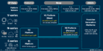
I wrote recently about the Arm v9 announcement, perhaps not a blockbuster but lots of new goodies. They have quickly followed with more of a blockbuster update on their Neoverse series. The product family that aims to address everything infrastructure-related, from cloud servers to communication backbones to the edge. Last year, Chris Bergey, Sr. VP and GM of Infrastructure detailed the product plan. V-series for maximum performance, N-series for scale-out performance and E-series for maximum throughput. This year he announced V-series and N-series updates along with a new and improved CMN (coherent mesh network).
V1 is the first introduction in the V-series and offers a 50% performance uplift (over plan I assume). It also supports 2x256b SVE (scalable vector extensions) and bfloat16. Per Google, bfloat16 is ideal in cloud applications, especially in TPUs. Take from that what you will.
N2 is the second release in the N-series, with a 40% performance uplift, also with SVE but here 2x128b, and again bfloat16.
CMN only rated one slide in the briefing but I know it will be integral to server architectures. Indeed any regular arrayed structure, though multi-core server chips are the most obvious application. The new CMN-700 supports more cores, caches, crosspoint nodes, memory ports and CCIX ports per die (they also support CXL).
Hyperscalar and supercomputing growth
Some big announcements here, starting with another leading hyperscalar adoption from Tencent (they’re already announced in support of cloud gaming). And Neoverse is coming soon to Oracle Cloud, here delivered by Ampere Altra processors. Good to see that Ampere is finding serious traction. The hyperscalar oligopoly needs external competition.
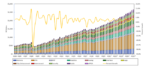
AWS Graviton2 is already available as an EC2 instance. AnandTech ran an analysis last year with comparison to the latest (and then not yet released) Intel and AMD processors. The comparison is clouded in mysteries of how AWS rate their EC2 instances, so difficult to draw black and white conclusions. But it’s telling that the Arm-based server is now being compared directly with top-of the line servers. And AWS shows that growth in EC2 instances is now dominated by Graviton instances.
Alibaba have tested their own Arm-based cloud instances, announcing a significant performance boost in a SPECjbb benchmark and a jump in their DragonWell Open Java development kit on N2 by 50%. I think I see a theme here. If you’re big in cloud, you’re building (or buying) Arm-based instances
Also the Ministry of Electronics and Information Technology (MeitY) in India is driving an exascale project under their center for development of advanced computing (C-DAC). This will leverage French SiPearl Rhea for servers (72 V1 cores, HBM2 and DDR5 memory, in TSMC 6nm). And South Korean ETRI K-AB21 (based on Arm Zeus, an earlier name for one of the Neoverse cores) for high performance and low power inference.
5G growth
Marvell has launched their OCTEON family addressing 5G RAN applications, with applications in remote radio units, distributed units and central units. Also to Smart NIC cards. All building on N2 cores
At the edge, Arm has been collaborating with Vodaphone on uCPE (universal customer premises equipment) which is – and I quote – “a general-purpose platform that integrates compute, storage and networking on a commodity, off-the-shelf server. This allows it to provide network services (such as SD WAN, firewall etc.) as virtual functions to any site on a network. uCPE is the equivalent of a ‘Cloud for network services’, but at the customer site.” Reducing total cost of ownership for the customer and reducing their carbon footprint.
Lots of good progress. You can read the release HERE.

