
Let me acknowledge up front that Avery isn’t the most visible EDA company around. If you know of them, you probably know their X-propagation simulator. Widely respected and used, satisfying a specialized need. They have also been quietly building over the years a stable of VIPs and happy customers, with a special focus on VIPs for PCIe and standards building on PCIe such as NVMe, CXL and CCIX. All hot standards in datacenters. Avery claims, and I have no reason to doubt them, that they are the #1 provider of VIPs in this area.
OK, good for them, they’re now active in a bigger market with more product range. But what caught my attention is what they are offering around CXL. First, I need to explain why this is important.
The off-chip cache coherence war
For those of you who don’t know, CXL and CCIX are off-chip/off-die cache-coherent interfaces. In some applications, particularly in machine learning, designs have become so big that they must split across multiple die/chips. Accelerators, memory and administration spread across multiple die. Yet applications still require the system as a whole to have a common logical view of memory. Which, since those memory accesses are mediated by caches, means they must be cache coherent. This problem has been solved on-chip through for example the ARM CCI network and the Arteris IP Ncore NoC. But those only work on-chip. CXL and CCIX extend from these networks to interconnect between chips/die. Intel is behind CXL, while AMD, ARM and several others are behind CCIX.
A new standards war, but what is important here is that, as I mentioned earlier, these standards are exceptionally important in datacenters. Particularly to the hyperscalars. And they’re still very new standards.
Avery CXL – more than a VIP
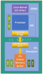
All of which means that compliance testing becomes very important. Against emerging/evolving standards. This takes a bit more than just VIPs, especially for cache coherence checking which must run through extensive testing. So Avery stepped up. They have built a virtual host co-simulation platform, around a CXL-aware QEMU emulator running Linux and connecting to a simulation (or emulation or prototyping platform) running the DUT. Avery’s CXL VIP sits inside the DUT testbench and connects to the QEMU host. Particularly notable here is that the VIP (and the QEMU host and Linux kernel with latest Intel patches for CXL) is ready to run type-3 designs, ahead of availability of processor silicon supporting that release.
This is arranged so the QEMU host looks like an Intel motherboard CXL host system. Meaning that a design team can validate against this setup. With high confidence that what they will build will work against real boards once those become available. In particular, they can run compliance tools and tests suites, such as CXLCV. And they can run performance benchmarking applications such as FIO and PCMark8.
Avery is contributing to the Intel QEMU/SystemC branch with a number of extensions in support of this capability. You might expect to see such a solution in compliance labs, especially since Avery is an early CXL Consortium member. And you probably wouldn’t be wrong.
And it’s more than CXL
Unsurprisingly, Avery also supports this path for PCIe host communication. They’ve recently been working with the University of New Hampshire Interoperability Lab and an industry leading NVMe SSD vendor on NVMe SSD validation using the UNH-IOL INTERACTTM test software. Plus other performance benchmarking applications such as FIO, PMark8, and CrystalDiskMark. Each of these comes which their own compliance tools you can run on the host side to model real traffic and testing against your DUT. The same QEMU co-sim idea also works for embedded processor side and supports Arm targets and AMBA bus communication.
Avery is now enabling more comprehensive validation of standards important to the hyperscalars and the companies who serve those giants. Leveling up indeed. You can learn more HERE.
Also Read:
Data Processing Unit (DPU) uses Verification IP (VIP) for PCI Express
PCIe 6.0, LPDDR5, HBM2E and HBM3 Speed Adapters to FPGA Prototyping Solutions


