
Throughout history, people have sought after security as a basic right and expectation within a civilized society. Even as recent as a few centuries ago, things were very simple. Subjects looked to their rulers to provide security for their lives and assets. Assets were mostly hard assets such as jewelry, coins or real estate. Administering security was simple and depended on strong guards who provided security through physical means.
Fast forward to today. Other than the house we live in and the vehicles we drive, most other assets are not physical in nature. Stocks, bonds, intellectual property ownership, fiat currencies, crypto currencies, etc. The list goes on. These assets are secured not by some physical means but rather through encryption and storage in the form of zeroes and ones in electronic form around the world. In other words, security is being provided through a combination of hardware/software solutions. For every security solution that is deployed, cyber criminals are always working to identify a weakness to break-in and steel assets.
Many of us know of or heard of mobile phone Subscriber Identity Module (SIM) cards getting cloned to perform unauthorized acts. The unauthorized act could be taking an Uber or Lyft ride under the guise of someone else. Or it could be a bigger act such as intercepting funds transfer that was meant for someone else, now that services exist to transfer monies based on mobile phone numbers. SIM card cloning is a security breach that all of us can relate to but is just one example to highlight the need for an unclonable solution.
It is in this context that eMemory Technology Inc. will be hosting a webinar that will be very informative and useful for chip designers and system engineers. The webinar is titled “PUFiot: A NeoPUF-based Secure Co-Processor” and is scheduled for June 8th, 2021 (EMEA time zones)/June 7th (Americas time zones). I got an opportunity to preview the webinar content. A number of things caught my attention. Following gives a peek into what to expect in the webinar. Please register for the webinar to learn all the intricate details.
Physical Unclonable Function (PUF)
A PUF can be thought of as a physically defined fingerprint and serve as a unique identify for a physical object. Although there are many different types of PUFs, the focus of the webinar is on PUFs implemented in semiconductors to uniquely identify a chip.
NeoPUF is Ideal PUF
NeoPUF is eMemory’s hardware security technology based on physically unclonable microvariations occurring in the silicon manufacturing process.
An ideal PUF is one that will enable the ultimate in security. For that, the PUF has to have the following characteristics.
Randomness: It has to be truly random and unpredictable
Uniqueness: Yet unique, so there is no duplication from device to device
Robustness: Should operate without errors over all PVT variations
Untraceability: Not provide a means for reverse engineering
Manufacturability: Reliably manufacturable with high yield
Radhard: Continue to function even under radiation exposure
The webinar goes into details of how all of the above characteristics are held by NeoPUF. For example, its true randomness results from the innovation of Quantum Tunneling, a world first. Users can generate truly random sequences for applications with high security requirements.
NeoPUF has also passed the NIST 800-22 test for ideal performance without the need for any data post-processing or data helpers such as error correction codes (ECC).
PUFiot
PUFiot is a high-security PUF-based crypto coprocessor to help chip designers easily adopt robust embedded hardware security functions. It has received the Cryptographic Algorithm Validation Program (CAVP) certification. CAVP is established by the National Institute of Standards and Technology (NIST) for technical verification. The certified security algorithms include AES, CMAC, DRBG, key wrap, SHA2, HMAC, KDF, and ECDSA.
This certification qualifies PUFiot under international security standards to meet the security needs of various application scenarios around the world.
Anti-tampering:
PUFiot provides a solid security boundary for chip protection through multiple analog/digital anti-tampering features built into the technology. It protects both intrusive attacks that may use focused ion beam methods and non-invasive attacks that may use side-channel analysis.
Zero-touch deployment:
By internally generating key pairs and IDs, PUFiot lowers the cost of supporting zero-touch deployment requirements of AI/IoT/5G multi-terabyte networked devices. Thus, it can assist cloud-based application ecosystems in achieving zero-trust compliant security operations.
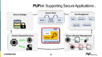
Supported Security Applications
The webinar covers how the PUFiot solution benefits IOT applications when implementing security. Security solutions need to comply with international security standards and regulations for different applications. The rapid growth in AI driven edge applications and related IoT devices demand anticlone measures. Refer to Figure below for the range of security applications that can benefit from a PUFiot-based solution.
Broad Support from Foundries
The NeoPUF technology and PUFiot co-processor IP are supported at TSMC, Samsung, UMC, GlobalFoundries SMIC and other foundries. The technology maintains high stability over a very wide temperature range (-40~175°C). It requires no additional mask layer and the IP can be implemented in a compact size for cost-effectiveness.
Summary
Anyone desiring to design non-clonable solutions for security applications would benefit a lot from attending this webinar. Register here for the “PUFiot: A NeoPUF-based Secure Co-Processor” webinar.

