Product Lifecycle Management (PLM) for electronic systems has moved from a passive ‘fire and forget’ approach to one that is intimately involved not only during design, but also throughout the entire life of every unit delivered to the field. Siemens EDA has a white paper titled “Tessent Silicon Lifecycle Solutions” that talks in depth about the advances in PLM that have come about due to a number of forces. Not only are their new requirements, but there are large potential benefits to customers and manufactures that can translate into significant economic upside.
The white paper posits that there are three drivers for semiconductor industry growth: technology scaling, design scaling and system scaling. PLM, with a new vision make it into a Silicon Lifecycle Solutions (SLS) platform, can address the needs created by each of these drivers. Technology scaling introduces the possibility of new types of silicon defects. It also adds to the likelihood of more early failures and wear-outs. Design scaling adds more gates and pins, with lower visibility into the internal operation of chips. System scaling leads to the inclusion of silicon into new applications such as transportation, server farms and others that add reliability, safety and security requirements.
Siemens EDA suggests a completely new way to look at what PLM in the form of a SLS platform can offer. In design and manufacturing, applying advanced DFT techniques and diagnosis driven yield analysis can reduce costs and improve time-to market for semiconductor companies. However, further down the supply chain, an SLS platform has the potential to help out OEM customers with fine grain data about the chip’s real-world performance and operation. We also know that for ISO 26262 applications in the automotive space that there needs to be continuous diagnostics to verify and ensure proper system operation. For data centers or high demand applications, gathering data on chip operation can help detect security issues or performance bottlenecks caused by failures or system level interactions.
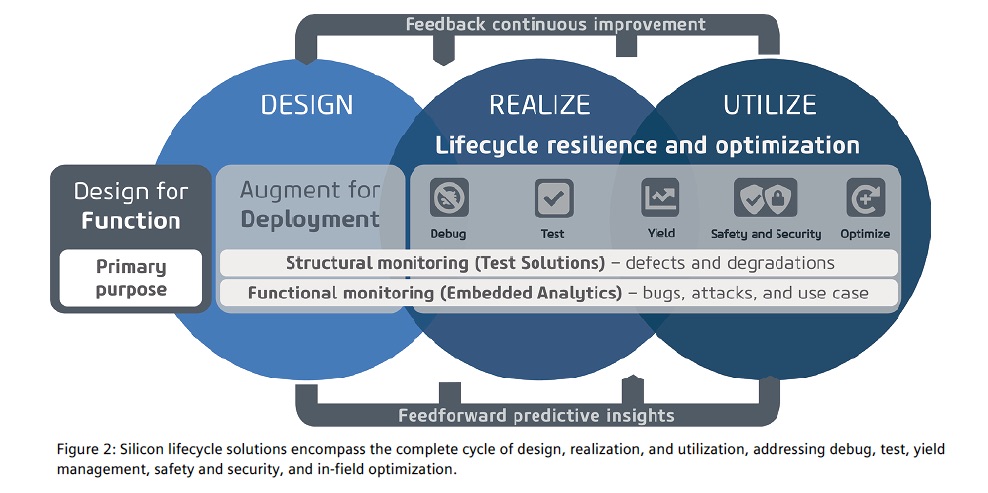
The Siemens EDA white paper articulates a vision for how a comprehensive SLS platform can be implemented to help gain the advantages mentioned above and others that can help with product development. Each stage of a product’s life cycle can be linked together providing feedback for continuous improvement and also forward predictive insights to improve system operation. This last point needs to be emphasized – a SLS platform has the potential to help optimize system performance in the field after installation.
What’s involved in implementing an SLS platform? At the front end there are on-chip resources, such as DFT logic and smart tools, parametric monitors and functional monitors to ensure that the hardware and software are operating as intended. In-system DFT and other monitors can produce prodigious amounts of data, so it is essential that there are tools to configure and manage these data streams. The Siemens SLS platform leverages tools that handle, process and correlate the data so it can be effectively used.

The white paper describes the Tessent SLS plaform with its four distinct layers. At the top it has software to assess, monitor and manage. Next is rapid analytics to help identify issues and their causes. Under this there is a database layer for managing the data from manufacturing, operation, and even databases for security with information to help identify cyber-attacks. The application layer has components that will be familiar to any hardware designer like DFT, BIST, and Tessent Diagnostics. It also ties into other domains such as safety analysis, predictive and preventive maintenance, security, and more.
The white paper discusses the details of how the Siemens SLS platform fulfills each of these layers. The Siemens Silicon Lifecycle Solutions platform is designed to provide all the parties in the design, manufacturing and deployment of semiconductor-based products with a means to ensure high quality, predictable reliability and efficient operation. We are seeing some of the anticipated benefits of Mentor’s acquisition by Siemens in the breadth and scope of this solution. The white paper is available on the Siemens EDA website.
Also Read:
Observation Scan Solves ISO 26262 In-System Test Issues
Siemens EDA wants to help you engineer a smarter future faster
Happy Birthday UVM! A Very Grown-Up 10-Year-Old
Share this post via:


Comments
There are no comments yet.
You must register or log in to view/post comments.