Synopsys 800x100 px High Quality

Alchip Reveals How to Extend Moore’s Law at TSMC OIP Ecosystem Forum

Alchip Reveals How to Extend Moore’s Law at TSMC OIP Ecosystem Forum
by Mike Gianfagna on 11-03-2021 at 10:00 am

Alchip Reveals How to Extend Moores Law at TSMC OIP Ecosystem Forum

The TSMC Open Innovation Platform (OIP) event brings together a wide array of companies reporting cutting edge work that are part of TSMC’s rather substantial ecosystem. The event covers everything from high-performance computing to mobile, automotive, IoT, RF and 3D IC design. Of particular interest for this post is a presentation made by Alchip. At the current incredible pace of innovation, methods to extend and enhance Moore’s law are of great interest to many. At the event, Alchip reveals how to extend Moore’s law with a targeted combination of technology and know-how. Read on to learn more.

Yield vs. number of die

The presentation was given by James Huang, vice president of R&D at Alchip Technologies. James began his presentation describing the yield challenges associated with a very large die at advanced technology nodes. As die size increases, yield decreases, sometimes approaching single-digit numbers. An alternative approach to address this issue is to segment the design into smaller portions, or chiplets and integrate the resulting pieces with advanced interface and packaging technology. A group of smaller chips, or chiplets will deliver a yield far better than a single, large die as shown in the figure.

James pointed out this approach does introduce additional costs from the advanced package, die to die interfaces and higher testing costs. The approach still delivers competitive total cost in many cases, however. There are several key ingredients required to make this approach viable. They include:

  • 2.5/3D packaging technology: TSMC 3DFabric™ & CoWoS® makes high bandwidth memory multi-die integration feasible.
  • Die-to-die communication: Alchip APLink (Advanced Package Link) D2D IOs enables high-speed data traffic between multiple chiplets.

James explained that Alchip’s APLink 4.0 is compatible with TSMC’s N3 process and offers a 16 Gbps line rate. It can use TSMC’s most advanced CoWos technology, offering five metal layers. An approach like this can definitely cut the large die yield issue down to size. This method of chip decomposition and reintegration is illustrated in the figure below.

2.5D package

He provided some information about APLink 4.0. Key features include:

  • Source-synchronous I/O bus running with standard core voltage
    • 12Tbps per PHY macro
    • 16Gbps per DQ line
    • 25+ pJ/bit
    • 5ns latency
  • Reliable system operation
    • De-skew, DBI
    • Eye training & monitoring
    • Lane repair
    • PVT monitoring

The APLink IP is delivered as a hard PHY macro with a soft controller. The IP supports south/north and east/west orientations. Symmetric PHY alignment achieves minimum die-to-die wire length. James then discussed the steps required to develop an effective chiplet-based design approach. Items to consider include:

  • Fundamentals
    • Process node selection for each chiplet
    • D2D IP performance and readiness
    • 5D/3D packaging lengthens the design cycle and introduces new risks
    • Total design and manufacturing cost
  • System architecture considerations
    • How to distribute sub-systems across multiple chiplets (chiplet partitioning)
    • Are power distribution networks sufficient?
    • Timing, thermal and SI/PI budgeting
    • Can individual chiplets be shut off?

As you can see, there is a lot to consider. James went on to point out other considerations, such as thermal dissipation, mechanical stress and warpage, and overall routing space for the interfaces. A lot of these issues must be considered early in the design process. These problems can be tamed, however. A successful 2.5D design was showcased during his presentation that contained multiple chiplets and HBM memory stacks.

He also discussed strategies for energy management for complex chiplet-based designs, as well as signal and power integrity considerations. Testing strategies for this kind of design were also discussed. Test can be quite a bit more complex when compared to a monolithic design.

James concluded with an overview of Alchip’s customer engagement model. The company works with the customer at every step in a collaborative way to ensure project success. If you are considering a chiplet-based approach for your next design, you should carefully consider your ASIC partner. There are many challenges with this type of design, and James demonstrated in his presentation a strong command of the requirements needed to achieve success.

You can learn more at www.alchip.com. You can also get lots of good information about Alchip on SemiWiki here, including a copy of the press release about the TSMC OIP presentation. And that is the story of how Alchip reveals how to extend Moore’s law with a targeted combination of technology and know-how.

Also Read:

Alchip is Painting a Bright Future for the ASIC Market

Maximizing ASIC Performance through Post-GDSII Backend Services

Alchip at TSMC OIP – Reticle Size Design and Chiplet Capabilities


Update on TSMC’s 3D Fabric Technology

Update on TSMC’s 3D Fabric Technology
by Tom Dillinger on 11-03-2021 at 8:00 am

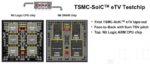
3D eTV testchip

TSMC recently held their 10th annual Open Innovation Platform (OIP) Ecosystem Forum.  An earlier article summarized the highlights of the keynote presentation from L.C. Lu, TSMC Fellow and Vice-President, Design and Technology Platform, entitled “TSMC and Its Ecosystem for Innovation” (link).

Overview of 3D Fabric

The TSMC 3D Fabric advanced packaging technology spans both the 2.5D and vertical die stacking offerings, as depicted below.

The Integrated FanOut (InFO) packages utilize a reconstituted wafer consisting of die embedded face down, surrounded by a molding compound (link).

Redistribution interconnect layers (RDL) are fabricated on the epoxy wafer.  (InFO-L refers to a silicon “bridge chiplet” between die embedded in the InFO package for improved inter-die connectivity over the RDL metallization pitch.)

The 2.5D CoWoS technology integrates die (and often, high-bandwidth memory stacks) on an interposer utilizing microbump attach.  The original CoWoS technology offering (now CoWoS-S) used a silicon interposer, and related silicon-based lithography for RDL fabrication;  through-silicon vias (TSVs) provide connectivity to the package bumps.  The silicon interposer technology offers improved interconnect density, critical for the high signal count HBM interface.  More recently, TSMC has been offering an organic interposer (CoWoS-R), providing a tradeoff between interconnect density versus cost.

The 3D SoIC offering provides vertical integration utilizing hybrid bonding between die pads.  The die may be oriented in face-to-face or face-to-back configurations.  TSVs provide connectivity through the (thinned) die.

InFO and CoWoS offerings have been in high-volume production for several years.  The recent innovations in CoWoS development relate to expanding the maximum silicon interposer dimensions to greater than the maximum reticle size to accommodate a larger number of die (especially, HBM stacks), stitching together the RDL interconnects.

The majority of Jim’s presentation covered advanced in SoIC development.

SoIC Testchip

TSMC shared results of a recent SoIC qualification test vehicle, as shown below.

The configuration used was the vertical bonding of an (N5) CPU die with an (N6) SRAM die, in a face-to-back topology.  (Indeed, a major CPU vendor has pre-announced plans for a vertical “last-level” SRAM cache die attached to a CPU using TSMC’s SoIC, to be available in 1Q2022.)

SoIC Design Flow

Jim presented a high-level design flow for vertical die integration, as shown in the figure below.

The flow requires concurrent focus on both top-down system partitioning into individual die implementations, plus early analysis of the thermal heat dissipation in the composite configuration, as highlighted above.

The discussion on thermal analysis highlighted the “chimney” nature of the low thermal resistance paths of the BEOL PDN and interconnect, compared to the surrounding dielectrics, as shown above.  Specifically, TSMC has collaborated with EDA vendors on improving the accuracy of the SoIC model discretization techniques, applying a more detailed mesh in specific “hotspot” areas initially identified with a coarse grid analysis.

TSMC also presented a methodology recommendation to incorporate thermal analysis results into the calculation of SoIC static timing analysis derate factors.  Much like on-chip variation (OCV) is dependent upon the distance spanned by (clock and data) timing paths, the thermal gradient for the SoIC paths is an additional derate factor.  TSMC reported that on-die temperature gradients for a path are typically ~5-10C, and a small flat derate timing margin for temperature should suffice.  For SoIC paths, large gradients of ~20-30C are feasible.  A flat derate to cover this range would be too pessimistic for paths with a small temperature difference – results of SoIC thermal analysis should be used for derate factor calculation.

SoIC Testing

The IEEE 1838 standardization effort pertains to the definition of die-to-die interface testing (link).

Much like the IEEE 1149 standard for boundary-scan chains on-die for package-to-package testing on a printed circuit board, this standard defines the control and data signal ports on each die for post-stack testing.  The primary focus of the standard is to exercise the validity of the face-to-face bonds and TSVs introduced during SoIC assembly.

Jim indicated that this definition is sufficient for low-speed I/Os between SoIC die, yet a more extensive BIST method will be required for high-speed I/O interfaces.

TSMC Foundation IP for SoIC – LiteIO

TSMC’s library development teams commonly provide general-purpose I/O cells (GPIOs) for each silicon process node.  For the die-to-die connections in SoIC configurations, where the driver loading is less, TSMC offers a “LiteIO” design.  As illustrated below, the LiteIO design focuses on optimizing the layout to reduce parasitic ESD and antenna capacitances, to enable faster datarates between die.

EDA Enablement

The figure below lists the key tool features recently developed in collaboration with major EDA vendors for the InFO and SoIC package technologies.

Summary

TSMC continues to invest heavily in 2.5D/3D advanced packaging technology development.  The key recent initiatives have focused on the methodology for 3D SoIC direct die attach – i.e., partitioning, physical design, analysis.  Specifically, early thermal analysis is a mandatory step.  Additionally, TSMC shared results of their SoIC eTV qualification testchip vehicle.  2022 is shaping up to see the rapid emergence of 3D SoIC designs.

-chipguy

Also read:

Highlights of the TSMC Open Innovation Platform Ecosystem Forum

Highlights of the TSMC Open Innovation Platform Ecosystem Forum


Back to Basics in RTL Design Quality

Back to Basics in RTL Design Quality
by Bernard Murphy on 11-03-2021 at 6:00 am

Deming min

Harry Foster waxes philosophical in a recent white paper from Siemens EDA, in this case on the origins of bugs and the best way to avoid them. Spoiler alert, the answer is not to make them in the first place or at least to flush them out very quickly. I’m not being cynical – that really is the answer though practice often falls short of ideal. Harry suggests we need to get back to basics in RTL design quality, and what better place to start than W. Edwards Deming, a founding father of Total Quality Management.

W. Edwards Deming

Quality must be designed in

This seems trite but it’s often the simple mistakes that bite us, like an out-of-range indexing error. Best case they slow down system level testing, worst case they make it through to silicon. It’s easy for us to believe that we are mostly infallible and what few mistakes we make will be caught in verification. But survey after survey proves that trivial mistakes still slip through, because we should know we left the mirage of exhaustive testing behind a long time ago.

Following Deming, we need to design quality in, not try to paste it on in verification. Harry proposes a 3-step process for design, based on a combination of design plus intent. The first step, Produce, starts with producing correct RTL by design (I assume we’re talking here about new IP or subsystems). The argument here is that bugs per line of code (LOC) are more or less constant at 15-50 bugs per thousand LOC irrespective of whether you are creating RTL, C++ or Javascript. The best way to create less bugs is therefore less lines of code, using a higher level of abstraction like SystemC /C++, Chisel or some other domain specific language.

Proving that intent is met

Since the method connects design and intent, the second step aims to prove in design that the intent is met. Harry’s suggestion here is particularly to leverage static and formal verification tools. We are designing quality in, so this is a task for RTL designers. Who already have access to a wide range of apps to simplify this analysis. They can find FSM deadlocks, arithmetic overflow possibilities and potential indexing errors. For possible domain crossing bugs, they can find metastability potential and other domain crossing errors which in many cases cannot be detected at all in simulation. Another possible source of errors is in X optimism and pessimism. The former may at least waste valuable time in system-level verification and the latter can create mismatches between RTL and gate-level sims which even equivalence checking may not find.

Your system verification team will thank you. Or they may curse you if they find problems you could have fixed before you checked in your code.

Protecting intent

The third pillar requires that intent should be protected through the rest of the design lifecycle by continued testing. Harry’s suggestion is to adopt a continuous integration (CI) flow here. We simply reuse the static and formal tests we developed and proved in design. These are largely hands-free and fast tests which should quickly flag checkin mistakes (we all make them).

A final (blogger) thought

This is a worth addition to the canon. We all nod wisely but we still trip up sometimes. With tools like CI we should be able to flush out more of these problems early on.

That said, there are some system-level problems which remain challenging, and which can’t be fixed (I think) at the unit-level. Cache coherence problems, emerging only after billions of cycles are one good example. Power bugs are difficult to cover fully in designs with very complex power and voltage switching. Security problems around speculative execution are another example. It would be great to find some kind of “unit test” methodologies around these system-level “IP”.

You can access the white paper HERE.

Also Read

APR Tool Gets a Speed Boost and Uses Less RAM

DARPA Toolbox Initiative Boosts Design Productivity

Heterogeneous Package Design Challenges for ADAS


On-Chip Sensors Discussed at TSMC OIP

On-Chip Sensors Discussed at TSMC OIP
by Tom Simon on 11-02-2021 at 10:00 am

phase noise correlation

TSMC recently held their Open Innovation Platform (OIP) Ecosystem Forum event where many of their key partners presented on their latest projects and developments. This year one of their top IP provider partners, Analog Bits, gave two presentations. Analog building blocks have always been necessary as enabling technology on leading edge designs. The move to 3nm continues this important relationship. Analog Bits has developed specialized analog IP that can help differentiate end products. For instance, they have focused on optimized high performance and low power SerDes, among other things. Another significant area is specialized on-chip sensors for monitoring chip health and performance.

In his presentation Mahesh Tirupattur, Analog Bits’ EVP, discussed how their sensing IP was used by Cerebras in developing the largest chip ever designed. The Cerebras WSE-2 has 2.6 trillion transistors in 850,000 optimized cores covering 46,225 square mm of silicon.  Cerebras faced challenges in power distribution and power supply integrity. Analog Bits IP offered them a solution to monitor chip operation in real time that can be used to apply real time corrective actions. They used 840 distributed glitch detectors to provide real time coverage of the entire design. The Analog Bits glitch detectors can detect short duration events that could otherwise easily be missed. They are programmable for trigger voltage, depth of glitch and time span of glitch. Their sensitivity exceeds 5pVs.

Recently Analog Bits expanded their sensor offering by adding power supply glitch detectors with an integrated voltage reference to their lineup of integrated POR sensors and on-die PVT sensors. This allows them to cover all aspects of chip operation in real time, including POR conditions – and now the health of the power supplies.

Of course, sensors require extremely high accuracy to correctly report chip behavior. Similarly, clocking macros need accuracy to enable proper chip operation. So, it was good to see that their second presentation at OIP was specifically on the topic of design and verification of these blocks. The paper was titled “Design and Verification of Clocking Macros and Sensors in N5 and N3 Processes Targeting High Performance Compute, Automotive, and IoT Applications”, and authored by Sweta Gupta, Director of Circuit Engineering at Analog Bits and Greg Curtis, Sr. Product Manager of Siemens EDA. The paper itself was the result of a three-way collaboration between TSMC, Siemens and Analog Bits.

In the second presentation Analog Bits shared correlation data on silicon measurements to specification for several of their PLLs, a power supply droop detector and a temperature sensor. Here is one of their slides on the phase noise correlation between measurement and silicon for a PLL built in TSMCs N5.

phase noise correlation

Analog Bits has a broad and well thought out portfolio of analog IP. They have customers on a wide range of processes from 0.25um to 3nm. I am sure that part of their success stems from their no-royalty business model. They have billions of units shipped from over a thousand IP deliveries since they first started in 1995. While the OIP presentations are over, more detailed information on all of their IP for on-chip sensors, SerDes, clocks and I/Os is available by contacting them. Their website offers detailed products listings & data sheets, and access to their N5 test chip video.

Also read:

Package Pin-less PLLs Benefit Overall Chip PPA

Analog Sensing Now Essential for Boosting SOC Performance

Analog Bits is Taking the Virtual Holiday Party up a Notch or Two


Design Technology Co-Optimization for TSMC’s N3HPC Process

Design Technology Co-Optimization for TSMC’s N3HPC Process
by Tom Dillinger on 11-02-2021 at 8:00 am

N3HPC performance comparison

TSMC recently held their 10th annual Open Innovation Platform (OIP) Ecosystem Forum.  An earlier article summarized the highlights of the keynote presentation from L.C. Lu, TSMC Fellow and Vice-President, Design and Technology Platform, entitled “TSMC and Its Ecosystem for Innovation” (link).

One of the topics that L.C. discussed was the initiatives that TSMC pursued for the N3 process node, specifically for the High-Performance Computing (HPC) platform.  This article provides more details about the design-technology co-optimization (DTCO) activities that resulted in performance gains for N3HPC, compared to the baseline N3 process.  These details were provided by Y.K. Cheng, Director, Design Solution Exploration and Technology Benchmarking, in his presentation entitled “N3 HPC Design and Technology Co-Optimization”. 

Background

Design technology co-optimization refers to a cooperative effort among process development engineering and circuit/IP design teams.  The technology team optimizes the device and lithography process “window”, typically using TCAD process simulation tools.  At advanced nodes, the allowed lithographic variability in line widths, spacings, uniformity, and density (and density gradient) is limited – technology optimization seeks to define the nominal fabrication parameters where the highly-dimensional statistical window maintains high yield.  The circuit design team(s) evaluate the performance impacts of different lithographic topologies, extracting and annotating parasitic R and C elements to device-level netlist models.

A key element to DTCO is pursued by the library IP team.  The standard cell “image” defines the allocated (vertical) dimension for nFET/pFET device widths and the number of (horizontal) wiring tracks available for intra-cell connections.  The image also incorporates a local power distribution topology, with global power/ground grid connectivity requirements.

In addition to the library cell image, the increasing current density in the scaled metal wires at advanced nodes implies that DTCO includes process litho and circuit design strategies for contact/via connectivity.  As the design variability in contact/via sizes is extremely limited due to litho/etch uniformity constraints, the process and circuit design teams focus on optimization of multiple, parallel contacts/vias and the associated metal coverage.

And, a critically important aspect of DTCO is the design and fabrication of the SRAM bitcell.  Designers push for aggressive cell area lithography, combined with device sizing flexibility for sufficient read/write noise margins and performance (with a large number of dotted cells on the bitlines).  Process engineers seek to ensure a suitable litho/etch window, and concurrently must focus on statistical tolerances during fabrication to support “high-sigma” robustness.

The fact that TSMC enables customers with foundation IP developed internally provides a tight DTCO development feedback loop.

N3HPC DTCO

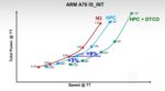
Y.K. began his presentation highlighting the N3HPC DTCO results, using the power versus performance curves shown in the figure below.  (The reference design block used for these comparisons is from an Arm A78 core;  the curves span a range of supply voltages, at “typical” device characteristics.)

The collective set of optimizations provide an overall 12% performance boost over the baseline N3 offering.  Note that (for the same supply voltage) the power dissipation increases slightly.

Y.K. went into detail on some of the DTCO results that have been incorporated into N3HPC.  Note that each feature results in a relatively small performance gain – a set of (consistent) optimizations is needed to achieve the overall boost.

  • larger cell height

Wider nFET and pFET devices within a cell provide greater drive strength for the (high-fanout) capacitive loads commonly found in HPC architectures.

  • increase in contacted poly pitch (CPP)

A significant parasitic contribution in FinFET devices is the gate-to-source/drain capacitance (Cgd + Cgs) – increasing the CPP increases the cell area (and wire lengths), but reduces this capacitance.

  • increased flexibility in back-end-of-line (BEOL) metal pitch (wider wires), with corresponding larger vias, as illustrated below
  • high-efficiency metal-insulator-metal (MiM) decoupling capacitor topology

The MiM capacitor cross-section illustrated below depicts three metal “plates” (2 VDD + 1 VSS) for improved areal efficiency over 2-plate implementations.

Improved decoupling (and less parasitic Rin to the capacitor) results in less supply voltage “droop” at the switching activity typically found in HPC applications.

  • double-height cells

When developing the cell image, the library design team is faced with a tradeoff between cell height and circuit complexity.  As mentioned above, a taller cell height allows for more intra-cell wiring tracks to connect complex multi-stage and/or high fan-in logic functions.  (The most demanding cell layout is typically a scannable flip-flop.)  Yet, a larger cell height used universally throughout the library will be inefficient for many gates.

The DTCO activities for N3HPC led TSMC to adopt a dual-height library design approach.  (Although dual-height cells have been selectively employed in earlier technologies, N3HPC adopted more than 400 new cells.)  This necessitated extensive collaboration with EDA tool suppliers, to support image techfile definition, valid cell placement rules, and auto-place-and-route algorithms that would successfully integrate single- and double-height cells within the design block.  (More on EDA tool features added for N3HPC shortly.)

As part of the N3HPC library design, Y.K. also highlighted that the device sizings in multi-stage cells were re-designed for optimized PPA.

  • auto-routing features

Timing-driven routing algorithms have leveraged the reduced R*C/mm characteristics of upper metal layers by “promoting” the layer assignment of critical performance nets.  As mentioned above, the N3HPC DTCO efforts have enabled more potential BEOL metal wire lithography width/spacing patterns.

As shown below, routing algorithms needed enhancements to select “non-default rules” (NDRs) for wire width/spacing.  (The use of NDRs have been available for quite a while – typically, these performance-critical nets were routed first, or often, manually pre-routed. The N3HPC DTCO features required extending NDR usage as a general auto-route capability.)  The figure also depicts how via pillar patterns need to be inserted to support increased signal current.

For lower metal layers where the lithography rules are strict and NDRs are not an option, routing algorithms needed to be enhanced to support parallel track routing (and related via insertion), as shown above.

EDA Support

To leverage many of these N3HPC DTCO features, additional EDA tool support was required.  The figure below lists the key tool enhancements added by the major EDA vendors.

Summary

TSMC has made a commitment to the high-performance computing platform, to provide significant performance enhancements as part of an HPC-specific process offering.  A set of DTCO projects were pursued for N3HPC, providing a cumulative 12% performance gain on a sample Arm core design block.  The optimizations spanned a range of design and process lithography window characteristics, from standard cell library design to BEOL interconnect options to MiM capacitor fabrication.  Corresponding EDA tool features – especially for auto-place-and-route – have been developed in collaboration with major EDA vendors.

For upcoming process node announcements – e.g., N2 – it will be interesting to see what additional DTCO-driven capabilities are pursued for the HPC offering.

-chipguy

Also read: Highlights of the TSMC Open Innovation Platform Ecosystem Forum


Yep – It’s Still an Analog World in this Digital Age

Yep – It’s Still an Analog World in this Digital Age
by Daniel Nenni on 11-02-2021 at 6:00 am

Fig 1 Omni Design Blog 271021

With all the advances in digital technology to serve mankind’s insatiable appetite for automation, it’s easy to lose sight of the reality that we still live in an analog world.  It’s easy to take for granted that somewhere in the chain of events that takes place in the process of applying state-of-the-art computational technology to real-world applications – data-conversion from analog to digital must take place.  Conversion of real-world information into a digitally encoded representation, and often back again to an analog representation.  Some are now claiming that we have evolved past the “digital age”, and we are now in the “age of data” – big data.

Sentient beings are largely algorithmic engines driven by the need to survive in a hostile environment – touch, vision, hearing, smell, taste (and sometimes “proprioception”). The human system converts our real-world senses into electrochemical “data” for processing by the brain’s neocortex to render our perception intelligence. As Artificial Intelligence (a.k.a. “AI”) promises to reshape our way of life beyond recognition, more data will be the key to better performing AI.  And, yes – I am referring to real-world data.  From online user data for better commercial transactions, to biosensor data for better healthcare, to real-time physical environment data for autonomous vehicle navigation.  In Kai-Fu Lee’s book “AI Super-Powers”, the use of real-world physical environment data by AI leads to what Kai-Fu refers to as perception AI – where AI-driven machines can “perceive their environment”.  And, clearly, high performance data-conversion will be a key ingredient for perception AI to achieve its full potential.

Omni Design Technologies is a leading provider of high-performance, ultra-low power data-conversion IP cores for SoCs that enable environment perception.  Specifically, Omni Design provides production-proven data-conversion IP that is more commonly known as ADCs (analog-to-digital converters), DACs (digital-to-analog converters), and AFEs (analog front-ends).  As you can easily imagine, ADCs, DACs, and AFEs are essential architectural components for any system that needs to interact with the real-world for environment perception – including those systems employing Light Detection and Ranging (“LiDAR”) technology.  LiDAR is making its way into a wide assortment of applications from the iPhone 12 Pro and iPhone 12 Pro Max with built-in LiDAR scanners for better photos and AR – to enabling vehicles with environment perception for autonomous navigation.

If the use of LiDAR in autonomous vehicles is your thing, Omni Design has recently published a white paper entitled “LiDAR Implementations for Autonomous Vehicle Applications”.  The white paper introduces LiDAR technology and discusses pulse-detection LiDAR as well as continuous-wave LiDAR.

Figure 1: Pulse-Detection LiDAR

Figure 2: FMCW LiDAR

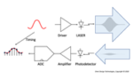
The white paper goes on to discuss several different implementations of LiDAR systems, SoC design requirements, and a block diagram example of a pulse-based LiDAR system SoC with available Omni Design IP.

Figure 3: Pulse-Based LiDAR Block Diagram

Finally, the white paper wraps up with a summary of Omni Design’s IP offering for implementing SoCs for LiDAR applications.

About Omni Design Technologies
Omni Design Technologies  is a leading provider of high-performance, ultra-low power IP cores in advanced process technologies that enable highly differentiated systems-on-chip (SoCs) in applications ranging from wired and wireless communications, automotive, imaging, sensors, and the internet-of-things (IoT). Omni Design, founded in 2015 by semiconductor industry veterans, has an excellent track record of innovation and collaborating with customers to enable their success. The company is headquartered in Milpitas, California with additional design centers in Fort Collins, Colorado, Billerica, Massachusetts and Bangalore, India. For more information, visit www.omnidesigntech.com.


Latest Updates to Altair Accelerator, the Industry’s Fastest Enterprise Job Scheduler

Latest Updates to Altair Accelerator, the Industry’s Fastest Enterprise Job Scheduler
by Mike Gianfagna on 11-01-2021 at 10:00 am

Latest Updates to Altair Accelerator the Industrys Fastest Enterprise Job Scheduler

Altair is a broad-based company that delivers critical enabling technology across many disciplines that will be familiar to SemiWiki readers. According to its website, Altair delivers open-architecture solutions for data analytics & AI, computer-aided engineering, and high-performance computing (HPC). You can learn more about Altair projects covered on SemiWiki here. Enterprise-level job scheduling is one example of the critical enabling technology Altair delivers. Recent, significant enhancements to the product are the subject of this post. Read on to learn about the latest updates to Altair Accelerator, the industry’s fastest enterprise job scheduler.

What It Is

Accelerator is a high-throughput, enterprise-grade job scheduler. Its application is focused on complex semiconductor design. The architecture is flexible and can support a variety of infrastructures from small, dedicated server farms to complex, distributed high-performance cluster environments.

A tool like this is needed by designers to allow for quick scheduling and resource management for their design tasks across CPU, memory and EDA license utilization. As compute infrastructures become more complex and distributed, there is also a growing need to manage resources to keep throughput high while managing overall costs. From a management perspective, there can be many thousands of jobs to schedule and prioritize each day – a tool with high visibility and low latency is needed to operate successfully in such an environment.

What’s New

This year, a native Kafka interface was added to enhance visualization across a broad range of information regarding batch scheduling for Accelerator. Information like this is notoriously difficult and costly to capture, so this enhancement is significant. Apache Kafka is an open-source tool for processing multiple sources of streaming data in real-time. Kafka is quite popular, with more than 80% of all Fortune 100 companies using it.

Monitoring of a high-performance batch system can be difficult. Most approaches typically slow down the system because of the reporting tasks, which compete with the tasks to process jobs.

It gets more difficult when there are several consumers of the monitored data. Slowing the refresh rate of monitor data can help, but then the information is not accurate or real-time.

A system such as Kafka helps by supporting many consumers. Data is published once but many consumers can read the message, so there is only one extra load on the batch system instead of many. For multiple clusters, multiple batch systems can be configured that publish to a single Kafka instance.

The frequency of data publishing does require care, even in this setting. How often should the system publish and how is the data extracted from the batch system? It’s important to understand how fast things are changing in the batch system. For example, Altair Accelerator can dispatch several hundred jobs per second, and each dispatch may change the state of 20-30 metrics. That’s a huge volume of data for just some basic measurements.

With its internal metrics system, Accelerator accumulates data over a short time window — around 10 seconds. While this loses resolution at the individual dispatch loop level, the resulting data is often more useful because of the high variance between dispatch loop iterations. Even with such accumulation, there’s still the overhead of getting the data out of the inner loop. Altair chose to directly code the Kafka publisher routines into the batch system core for lower overhead.

To Learn More

The results of the enhancements to Altair Accelerator are significant. You can get more information and view sample reports here. You can also see a short demonstration of the new Accelerator dashboard here. There are also great examples of enhanced data streams that are now possible with the new release here.  This information will help you learn about the latest updates to Altair Accelerator, the industry’s fastest enterprise job scheduler.

Also Read

Six Essential Steps For Optimizing EDA Productivity

Chip Design in the Cloud – Annapurna Labs and Altair

Webinar: Annapurna Labs and Altair Team up for Rapid Chip Design in the Cloud


Highlights of the TSMC Open Innovation Platform Ecosystem Forum

Highlights of the TSMC Open Innovation Platform Ecosystem Forum
by Tom Dillinger on 11-01-2021 at 8:00 am

N3 comparison

TSMC recently held their 10th annual Open Innovation Platform (OIP) Ecosystem forum.  The talks included a technology and design enablement update from TSMC, as well as specific presentations from OIP partners on the results of recent collaborations with TSMC.  This article summarizes the highlights of the TSMC keynote from L.C. Lu, TSMC Fellow and Vice-President, Design and Technology Platform, entitled: “TSMC and Its Ecosystem for Innovation”.  Subsequent articles will delve more deeply into specific technical innovations presented at the forum.

TSMC OIP and Platform Background

Several years ago, TSMC defined four “platforms”, to provide specific process technology and IP development initiatives aligned with the unique requirements of the related applications.  These platforms are:

  • High-Performance Computing (HPC)
  • Mobile (including, RF-based subsystems)
  • Automotive (with related AEC-Q100 qualification requirements)
  • IoT (very low power dissipation constraints)

L.C.’s keynote covered the recent advances in each of these areas.

OIP partners are associated with five different categories, as illustrated in the figure below.

EDA partners develop new tool features required to enable the silicon process and packaging technology advances.  IP partners design, fabricate, and qualify additional telemetry, interface, clocking, and memory IP blocks, to complement the “foundation IP” provided by TSMC’s internal design teams (e.g., cell libraries, general purpose I/Os, bitcells).  Cloud service providers offer secure computational resources for greater flexibility in managing the widely diverse workloads throughout product design, verification, implementation, release, and ongoing product engineering support.  Design center alliance (DCA) partners offer a variety of design services to assist TSMC customers, while value chain aggregation (VCA) partners offer support for test, qualification, and product management tasks.

The list of OIP partners evolves over time – here is a link to an OIP membership snapshot from 2019.  There have been quite a few recent acquisitions, which has trimmed the membership list.  (Although not an official OIP category, one TSMC forum slide mentioned a distinct set of “3D Fabric” packaging support partners – perhaps this will emerge in the future.)

As an indication of the increasing importance of the OIP partner collaboration, TSMC indicated, “We are proactively engaging with partners much earlier and deeper (my emphasis) than ever before to address mounting design challenges at advanced technology nodes.”       

Here are the highlights of L.C.’s presentation.

N3HPC

In previous technical conferences, TSMC indicated that there will be (concurrent) process development and foundation IP releases focused on the HPC platform for advanced nodes.

The figures below illustrate the PPA targets for the evolution of N7 to N5 to N3.  To that roadmap, TSMC presented several design technology co-optimization (DTCO) approaches that have been pursued for the N3HPC variant.  (As has been the norm, the implementation of an ARM core block is used as the reference for the PPA comparisons.)

Examples of the HPC initiatives include:

  • taller cells, “double-high” standard cells

N3HPC cells adopt a taller image, enabling greater drive strength.  Additionally, double-high cells were added to the library.  (Complex cells often have an inefficient layout, if confined to a single cell-height image – although double-high cells have been used selectively in previous technologies, N3HPC adopts a more diverse library.)

  • increasing the contacted poly pitch (CPP)

Although perhaps counterintuitive, increasing the cell area may offer a performance boost by reducing the Cgs and Cgd parasitics between gate and S/D nodes, with M0 on top of the FinFET.

  • an improved MiM decoupling capacitance layout template (lower parasitic R)
  • greater flexibility – and related EDA auto-routing tool features – to utilize varied (wider width/space) pitches on upper-level metal layers)

Traditionally, any “non-default rules” (NDRs) for metal wires were pre-defined by the PD engineer to the router (and often pre-routed manually);  the EDA collaboration with TSMC extends this support to decisions made automatically during APR.

Note in the graph above that the improved N3HPC performance is associated with a slight power dissipation increase (at the same VDD).

N5 Automotive Design Enablement Platform (ADEP)

The requirements for the Automotive platform include a more demanding operating temperature range, and strict reliability measures over an extended product lifetime, including:  device aging effects, thermal analysis including self-heating effects (SHE), and the impact of these effects on electromigration failure.  The figure below illustrates the roadmap for adding automotive platform support for the N5 node.

Cell-aware internal fault models are included, with additional test pattern considerations to reduce DPPM defect escapes.

RF

RF CMOS has emerged as a key technology for mobile applications.  The figure below illustrates the   process development roadmap for both the sub-6GHz and mmWave frequency applications.  Although N16FFC remains the workhorse for RF applications, the N6RF offering for sub-6GHz will enable significant DC power reduction for LNAs, VCOs, and power amplifiers.

As for the Automotive platform, device aging and enhanced thermal analysis accuracy are critical.

N12e sub-Vt operation

A major initiative announced by L.C. related to the IoT platform.  Specifically TSMC is providing sub-Vt enablement, reducing the operating supply voltage below device Vt levels.

Background – Near-Vt and Sub-Vt operation

For very low power operation, where the operating frequency requirements are relaxed (e.g., Hz to kHz), technologists have been pursuing aggressive reductions in VDD – recall that active power dissipation is dependent upon (VDD**2).

Reducing the supply to a “near-Vt” level drops the logic transition drive current significantly;  again, the performance targets for a typical IoT application are low.  Static CMOS logic gates function at near-Vt in a conventional manner, as the active devices (ultimately) operate in strong inversion.  The figure below illustrates the (logarithmic) device current as a function of input voltage – note that sub-Vt operation implies that active devices will be operating in the “weak inversion” region.

Static, complementary CMOS gates will still operate correctly at sub-Vt levels, but the exponential nature of weak inversion currents introduces several new design considerations:

  • beta ratio

Conventional CMOS circuits adopt a (beta) ratio of Wp/Wn to result in suitable input noise rejection and balanced RDLY/FDLY delays.  Commonly, this ratio is based on the strong inversion carrier mobility differences between nFET and pFET devices.  Sub-Vt circuit operation depends upon weak inversion currents, and likely requires a different approach to nFET and pFET device sizing selections.

  • sensitivity to process variation

The dependence of the circuit behavior on weak inversion currents implies a much greater impact of (local and global) device process variation.

  • high fan-in logic gates less desirable

Conventionally, a high ratio of Ion/Ioff is available to CMOS circuit designers, where Ioff is the leakage current through inactive logic branches.  In sub-Vt operation, Ion is drastically reduced;  thus, the robustness of the circuit operation to non-active leakage current paths is less.  High fan-in logic gates (with parallel leakage paths) are likely to be excluded.

  • sub-Vt SRAM design considerations

In a similar manner, the leakage paths present in an SRAM array are a concern, both for active R/W cell operation and inactive cell stability (noise margins).  In a typical 6T-SRAM bitcell, with multiple dotted cells on a bitline, leakage paths are present through the access transistors of inactive word line rows.

A read access (with pre-charged BL and BL_bar) depends on a large difference in current on the complementary bitlines through only the active word line row array locations.  In sub-Vt operation, this current difference is reduced (and also subject to process variations, as SRAMs are often characterized to a high-sigma tail of the statistical distribution curve).

As a result, the number of dotted cells on a bitline would be extremely limited.  The schematic on the left side of the figure below illustrates an example of a modified (larger) sub-Vt SRAM bitcell design, which isolates the read operation from the cell storage.

  • “burst mode” operation for IoT

IoT applications may have very unique execution profiles.  There are likely long periods of inactivity, with infrequent “burst mode” operations requiring high performance for a short period of time.  In conventional CMOS applications, the burst mode duration is comparatively long, and a dynamic-voltage frequency-scaling (DVFS) approach is typically employed by directing a DC-to-DC voltage regulator to adjust its output.  The time required for the regulator to adapt (and the related power dissipation associated with the limited regulator efficiency) are rather inconsequential for the extended duration of the typical computing application in burst mode.

Such is not the case for IoT burst computation, where power efficiency is utmost and the microseconds required for the regulator to switch is problematic.  The right hand side of the figure above depicts an alternative design approach for sub-Vt IoT CMOS, where multiple supplies are distributed and switched locally using parallel “sleep FETs” to specific blocks.  A higher VDD would be applied during burst mode, returning to the sub-Vt level during regular operation.

TSMC is targeting their initial sub-Vt support to the N12e process.  The figure below highlights some of the enablement activities pursued to provide this option for the IoT platform.

TSMC hinted that the N22ULL process variant will also receive sub-Vt enablement in the near future.

L.C. also provided an update on the TSMC 3D Fabric advanced packaging offerings – look for a subsequent article to review these technologies in more detail.

Summary

TSMC provided several insights at the recent OIP Ecosystem forum:

  • HPC-specific process development remains a priority (e.g., N3-HPC).
  • The Automotive platform continues to evolve toward more advanced process nodes (e.g., N5A), with design flow enhancements focused on modeling, analysis, and product lifetime qualification at more stringent operating conditions.
  • Similarly, the focus on RF technology modeling, analysis, and qualification continues (e.g., N6RF).

and, perhaps the most disruptive update,

  • The IoT platform announced enablement for sub-Vt operation (e.g., N12e).

-chipguy

Also read: Design Technology Co-Optimization for TSMC’s N3HPC Process


Lecture Series: Designing a Time Interleaved ADC for 5G Automotive Applications

Lecture Series: Designing a Time Interleaved ADC for 5G Automotive Applications
by Kalar Rajendiran on 11-01-2021 at 6:00 am

Slide AMS Lecture Series Snapshot

A recent educational virtual event with the above title was jointly sponsored by Synopsys and Global Foundries. The objective was to bring awareness to state-of-the-art mixed-signal design practices for automotive circuits. The 2-day event comprised of lectures delivered by engineering professors and doctoral students from Wayne State University. The lecture series focused on designing a time interleaved ADC for 5G V2X automotive applications.

If you were not available to attend the live virtual event, you can now listen to the lectures on-demand. This blog provides a backdrop for the lecture series and a brief overview of the lectures.

Automotive Industry

The automotive industry ecosystem has been working on a vehicle-to-everything (V2X) communication system to support autonomous vehicles. The primary purpose of a V2X system is to improve road safety, enhance road traffic efficiency and bring energy savings to automobiles. As such, in addition to the usual requirements of performance, power, area and cost, field reliability of the implemented integrated circuits becomes imperative. As a result, IC designers must ensure that their designs are fail-operational, have low defect rates, and operate reliably over a long period of time.

Lectures Series Overview

You will learn how to design and verify a time-interleaved ADC targeted for 5G V2X application using Global Foundries 22nm FDSOI process technology. You will also learn about the Global Foundries FDSOI process technology. This is the process technology that is used to implement the ADC during this analog-mixed-signal (AMS) lecture series. The lectures cover radio transceiver architecture for V2X systems, ADC architecture, ADC design and related challenges, layout and related changes, accounting for post-layout parasitics, and aging effects.

Why Focus on Time Interleaved SAR ADC?

A complete V2X communication system has four subsystems to it, namely, vehicle-to-vehicle (V2V), vehicle-to-infrastructure (V2I), vehicle-to-pedestrian (V2P) and vehicle-to-network (V2N) communications. The complete system requires transceivers with two different specifications. This would lead to high cost and large chip area to implement the system and will also consume a high amount of power. The WINCAS Research Center at Wayne State University was already working on a single transceiver that can support all V2X applications.

The transceiver architecture is based on frequency planning and programmable ADCs. This means that the ADC has to deal with two different channel bandwidths. For V2V/V2P/V2I, the ADC input bandwidth is 75MHz with sampling frequency at 150MHz. For V2N, the ADC input bandwidth is 400MHz with sampling at 800MHz.

This frequency planning approach offers many benefits, some of which are:

    • maximum hardware sharing while covering all bands of V2X
    • PLLs achieving good phase noise at much reduced current consumption

While the benefits are very attractive, the architecture is the first of its kind, bringing with it its share of challenges to overcome. The ADC plays a critical role in this architecture, making it a suitable circuit to showcase state-of-the-art AMS circuit techniques through a lecture series.

Time Interleaved SAR ADC

The Time Interleaved ADC designed during this lecture series uses 8 channels. Each channel is a SAR ADC. Each SAR ADC has a DAC inside which has a comparator and track and hold. Before diving into the ADC design, the lectures present an improved version of track and hold circuit to avoid the typical issues with traditional implementations. Conventional implementations of track and hold circuits could lead to breakdowns due to over stress voltage conditions. They could also lead to incorrect bit conversions as a result of voltage changes on the top plate of the DAC inside the comparators. The lectures also discuss selection of capacitors for the DAC in order to handle thermal noise.

Design and Layout Challenges

Time Interleaved SAR ADCs are exposed to common mode noise and are sensitive to many types of errors. One such error is the clock skew error. The lecture discusses how to mitigate time skew through the use of dummy logic circuits and offers design techniques to eliminate common mode noise.

AMS designs experience noisy interaction between digital and analog portions of the circuitry. Major sources of this noise are capacitive coupling and power supply lines. Another source is lateral coupling between metal lines that run parallel. Floor plan techniques are presented to help minimize these kinds of situations during the physical routing.

Robustness of SAR ADC

Process, temperature and voltage (PVT) do affect the performance of an ADC. Given this circuit is for an automotive application, validating the design robustness across PVT is very critical. Robustness of a circuit in this regard means that it has a high probability of operating correctly even under conditions outside the specification. Results of corners simulations are presented showing that the performance of the SAR ADC is robust across all corners at different temperatures to meet the AEC-Q100 Grade 1 standard.

Aging and Electromigration

Aging and electromigration triggered faults are very key concerns for automotive applications. The choice of FD-SOI process for implementing the SAR ADC seems to be a good one in this regard. Not only does this process offer FinFET like performance with energy efficiency, it also allows for electrostatic control of the channel via body biasing. This allows for compensating for the static process variations and the dynamic temperature and aging variations.

FD-SOI is the only process technology to bring together three substantial characteristics of CMOS transistors:

  • 2D planar transistor structure
  • Fully depleted operation
  • Capability to dynamically modify the threshold voltage of transistors after manufacturing

Summary

It may be worthwhile for anyone involved in the development of V2X systems to register and listen to these lectures to learn some new circuit techniques. Below is a screenshot showing the different topics covered over a series of nine lectures. You can listen to the lectures in any order or just the ones that are of interest to you. Access the lecture series on-demand from here.

Also read:

Synopsys’ ARC® DSP IP for Low-Power Embedded Applications

Synopsys’ Complete 800G Ethernet Solutions

Safety + Security for Automotive SoCs with ASIL B Compliant tRoot HSMs


SISPAD – Cost Simulations to Enable PPAC Aware Technology Development

SISPAD – Cost Simulations to Enable PPAC Aware Technology Development
by Scotten Jones on 10-31-2021 at 10:00 am

Slide11

I was invited to give a plenary address at the SISPAD conference in September 2021. For anyone not familiar with SISPAD it is a premiere TCAD conference. This year for the first time SISPAD wanted to address cost and my talk was “Cost Simulations to Enable PPAC Aware Technology Development”.

For many years the standard in technology development has been Power, Performance and Area (PPA), for example: on TSMC 2020-Q4 earnings call, N3 will have 30% lower power at the same performance (Power), 15% greater performance at the same power (Performance) and 70% greater density (Area).

More recently increasing wafer costs are driving the need to add cost as PPAC, Power, Performance, Area and Cost. Companies such as TSMC at IEDM 2019 [1], Imec at their technology forum in 2020 [2] and Applied Materials at SEMICON West in 2020 [3], and many others are all taking about PPAC.

The current practice when developing a new technology is to define initial PPA targets, identify designs for PPA evaluation, select a transistor architecture, develop an initial process flow, simulate transistor performance, and extract a SPICE model, select a standard cell architecture, and generate a cell library. The cell library and process flow are then fed into a Design Technology Co Optimization simulation suite such as is offered by Synopsys to simulate the process, generate a 3D structure, and extract the parasitic netlist. The library can then be characterized, a physical design can be done and PPA can be evaluated. The PPA is then evaluated, and the designed experiment iterations can be done to achieve the PPA targets all in a simulation environment. What is missing in this process is any cost awareness. If the ability to simulate cost is added to a DTCO suite then the process can target PPAC, and iterations can be done in a simulation environment to achieve the PPAC targets.

To accurately simulate costs both the facility running the process and the process must be considered. The same process in two different facilities will have different costs, sometimes significantly different. Two different processes run in the same facility will have different costs, sometimes significantly different.

Facility Cost

The designed capacity of a fab has a significant impact on cost. There is a wide variety of throughputs for fab equipment and the higher the fab design capacity the better the capacity matching of the equipment set can be achieved. This results in higher capital efficiency and therefore lower cost per wafer for higher capacity fabs. Figure 1. Illustrates the normalized wafer cost versus capacity for a greenfield fab running a 5nm process in Taiwan.

Figure 1. Wafer cost versus fab capacity.

 The country a fab is in also impacts the cost. Figure 2 compares the same fab described above designed for 40,000 wafers per month in six different countries. The costs in figure 2 are operating costs only and do not include any incentives.

Figure 2. Wafer cost versus country.

Another critical cost factor is the age of the fab. For a new fab depreciation can represent over 60% of the cost of making a wafer. Figure 3 illustrates the same fab previously described for five different time frames:

  1. the first year ramping up (assuming 50% utilization on average).
  2. Years two through five when the fab is ramped up but the equipment is still depreciating.
  3. Year six when the equipment is depreciated.
  4. Year eleven when the facility systems are depreciated.
  5. Year sixteen when the building shell is depreciated.

Figure 3. Wafer cost versus fab age.

Accurate cost modeling requires the ability to define the fab capacity, country, and age.

Process Cost

Process costs begin with the starting wafer or wafers cost. Modeling needs to account for whether the starting wafer is a polished wafer, Epi wafer, or specialty wafer such as some kind of SOI. Also modeling needs to allow for more than one wafer, for example for processes where two wafers may be used and then bonded together.

Direct labor costs are the cost for operators to process the wafers. In current generation 300mm fabs there are every few operators because the wafer transport systems lower the front opening unified pods (FOUPs) right onto the tool but there are some operators. The labor hours required for a particular flow most be calculated, and the appropriate labor rate applied depending on the country where the fab is located.

Depreciation is the largest single cost in wafer fabrication, for new processes representing over 60% of the wafer cost (see figure 6 below). Accurate depreciation estimates require determining the equipment required and throughput for every step in the process flow. An accurate model needs to determine the appropriate generation of equipment for a process, the throughput, equipment cost, and physical space needed for the equipment and building a complete set for a target capacity. An accurate model should have background tables of equipment cost and configuration by node and construction costs for cleanroom space to enable detailed capital cost calculations.

Equipment maintenance costs include the costs for equipment parts that are consumed during processing such as quartz rings used in etch chambers, repair parts to replace equipment sub systems that break during operation of the equipment, and finally equipment service contracts. All these costs need to be estimated for the equipment set determined during the depreciation calculations.

Indirect labor costs encompass engineers and technicians that maintain the process and equipment, supervisors that manage the direct labor and managers that oversee everything. Headcounts need to be estimated and salaries by country and year applied.

Facility costs include electricity, water and sewer, ultrapure water generation, natural gas, facility maintenance, occupancy costs and insurance. Many of these costs depend on the country as well as year. An accurate model needs to have background tables by country and year and algorithms to perform the calculations.

Consumables are made up of hundreds of different materials consumed by the process (these are distinct from the equipment parts consumed during processing accounted for in equipment maintenance). Process materials include things like bulk gases, CVD and ALD precursors, CMP consumables, PVD targets, photoresist and reticles and many other items. An accurate model needs to have costs by year for thousands of target materials by year and calculate material usage by process step.

Commercial Implementation

IC Knowledge is the world leader and cost and price modeling for semiconductors and has recently developed process simulation technology to enable step by step process definition and cost estimation (Cost Explorer). Synopsys is a world leader in TCAD tools for technology development and simulation. IC Knowledge and Synopsys have partnered to embed IC Knowledge’s Cost Explorer in Synopsys Process Explorer tool that is used to simulate the physical structure produced by target process flow. Cost Explorer plug in for Process Explorer will enable users of Synopsys DTCO suite to define PPAC targets and design processes to meet those targets in a virtual environment utilizing designed experiments to optimize for all four elements of PPAC simultaneously.

Figure 4 illustrates the IC Knowledge – Synopsys solution.

Figure 4. Commercial PPAC TCAD Solution.

The current timeline for this solution:

  • Current status – beta testing at one customer with customer developed script to automatically populate Cost Explorer from Process Explorer. Beginning to show the capability to select customers.
  • End of 2021 – external cost model with script (Synopsys script) to populate Cost Explorer from Process Explorer.
  • Mid 2022 – fully implemented Process Explorer plug-in and commercial availability.

Customer Examples

As mentioned in the previous section we have customer beta testing the solution. The customer is a large OEM who uses Synopsys’ DTCO solution for technology development. The customer is developing Complementary FET (CFET) processes as a next generation solution beyond FinFETs and Horizontal Nanosheets (HNS).

Figure 5 illustrates the wafer cost broken out by category for a possible process flow. In the actual model the results are all in dollars and represent a specific fab and process configuration.

Figure 5. Wafer Cost by Category.

The OEM wanted to evaluate how CFET costs compared to FinFETs. They compared a standard FinFET, a FinFET with a Buried Power Rail (BPR) (BPR enables better density), a monolithic CFET with BPR and a sequential CFET where the CFET process is split between two wafer that are then bonded together, once again, in the actual model the results are all in dollars.

Figure 6. Normalized Wafer Cost Versus Process.

 The key conclusion from figure 6 is the OEM developed CFET process with BPR is competitive on cost to a FinFET process with BPR. Because CFETs stack the nFET and pFET devices they offer significant density improvements over FinFETs.

Another conclusion from figure 6 is the monolithic CFET process is less expensive than the sequential CFET process. The monolithic CFET process developed by the OEM is highly self-aligned and cost optimized.

While doing this work the OEM also evaluated lithography options for local interconnect comparing two solutions:

  1. EUV local interconnect mandrel mask with EUV cut, and EUV via mask.
  2. EUV local interconnect mandrel mask with multipatterned DUV cut, and EUV via mask.

Because the multipatterned cut can be implemented with a relatively simple multi-patterning scheme they found they could save $52 although there would be some cycle time impact.

Conclusion

The accelerating cost increases to fabricate leading edge wafers are driving the need to switch from PPA based technology development to PPAC based technology development. The partnership of IC Knowledge and Synopsys will for the first time provide the industry with the ability to design for PPAC in a virtual environment before ever running wafers. This capability will be a game changer for the industry and enable the continued evolution of Moore’s law.

References

[1] Geoffrey Yeap of TSMC during Applied Materials IEDM 2019 panel “Logic: EUV is Here , Now What?, “Power Performance Area Cost Time – PPACT where new technologies need to be on-time”.

[2] Luc Van Den Hove, President and CEO of Imec, Imec Technology Forum 2020, “Technologies for People in the New Normal,” slide 45, “Scaling Roadmap” “Power – Performance – Area – Cost”.

[3] Applied Materials, “Selective Gap Fill Announcement,” SEMICON West 2020, slide 2, “Power, Performance, Area-Cost” also including t for time to market.

Also Read:

TSMC Arizona Fab Cost Revisited

Intel Accelerated

VLSI Technology Symposium – Imec Alternate 3D NAND Word Line Materials