Synopsys 800x100 px High Quality

Losing Lithography: How the US Invented, then lost, a Critical Chipmaking Process

Losing Lithography: How the US Invented, then lost, a Critical Chipmaking Process
by Craig Addison on 10-31-2021 at 8:00 am

Lithography pioneers Perkin Elmer and Mann Co SEMI image

Lithography is arguably the most important step in semiconductor manufacturing. Today’s state-of-the-art EUV scanners are incredibly complex machines that cost as much as a new Boeing jetliner.

From humble beginnings in 1984 as a joint venture with Philips, ASML has grown to become the world’s second largest chip equipment maker – and the only supplier of EUV machines.

“Losing Lithography”, an episode in The Chip Warriors podcast series, provides a first hand account of how the US invented, then lost, this critical part of the chipmaking process. The episode is based on interviews with pioneers at Fairchild Semiconductor, David W Mann Co, Cobilt, GCA, Nikon and Silicon Valley Group (SVG), among others.

Early attempts to print images onto silicon wafers were undertaken at Bell Labs in the mid 1950s. Later that decade, Fairchild improved the process in order to make transistors.

“We decided to use photo resist in order to delineate the areas,” said Jay Last, one of the original eight co-founders of Fairchild, along with Bob Noyce.

“Bell Labs had made some efforts there and thought this was just impossible to work with so they never pursued it. Bob [Noyce] and I worked with Kodak and they gave us the best resists they had at the time and we gradually had a working relationship with them that resists kept steadily improving.

“There were a lot of technical problems and technical setbacks, but we just said we are going to use this and we have to make it work — and we did.”

In the 1960s contact mask aligners were used for wafer printing, with Kulicke & Soffa the first to introduce them commercially. Later, Kasper Instruments became the dominant supplier, but when three former Kasper engineers formed their own company, called Cobilt — and it was acquired by Boston-based CAD giant Computervision in 1972 — a new paradigm for wafer printing emerged.

“Cobilt made mechanical aligners that printed the semiconductor wafer with somewhat superior technology to the standard of the day. And Computervision had a package of automatic alignment which would allow you to align the layers more exactly,” said Sam Harrell, who moved from  Computervison to the West Coast to be Cobilt’s vice president of engineering.

“We sold hundreds of machines all over the world. It really reigned until the period of the projection printers became dominant.”

Ed Segal, who sold aligners at Kasper before joining Cobilt, saw how Cobilt lost its lead when Perkin-Elmer developed the projection mask aligner.

“When the mask aligner went to the next stage from a contact mask aligner to what was called a projection aligner, or projecting the image of the mask on the wafer, Perkin-Elmer just absolutely came in and took that market over,” Segal said. “Cobilt attempted to build one and it was really a very big failure. And the company eventually was sold to Applied Materials in 1981.”

Jim Gallagher ran the semiconductor equipment business at GCA, which was the world leader in lithography before ceding the market to Japanese companies in the 1980s. In the podcast, he recounts the eventual demise of the company after Japanese suppliers like Nikon and Canon became market leaders.

“We started to sell off operations as best we could. But when you’re going downhill, so to speak, that’s not the time to start selling because what you’re doing is, everybody knows your problem and they’re going to give the lowest, lowest prices. So that was the beginning of our slide,” Gallagher said.

By the late 1980s, the dominance of Japanese stepper suppliers was a worry for American chipmakers. In an effort to develop an alternative source, Intel worked with Censor, a European company. However, the effort failed and Censor was sold to Perkin-Elmer in 1984.

Intel co-founder Gordon Moore recalls the concern at the time. “The big steppers were coming out of Canon and Nikon. There wasn’t a comparable piece of equipment in the US, and that was such a critical part of the entire process.

“We had a major program with a Liechtenstein company [Censor] to make a stepper. Very sophisticated but also very expensive, and the development went too slowly for them to really make an impact on the market. We ended up buying Japanese equipment because it was the best available, and there wasn’t really an alternative source for that.”

Shoichiro Yoshida, who would later become CEO of Nikon, designed the company’s first step-and-repeat camera for semiconductor manufacturing. In the podcast, hear him describe (in English) the early development of steppers at Nikon.

In the 1990s, SVG expanded into lithography under newly appointed CEO Papken Der Torossian. SVG had tried to buy GCA but the deal never materialized, and GCA was sold to General Signal in 1988.

However, Der Torossian was successful in acquiring a next generation step-and-scan system, Micrascan, developed by Perkin-Elmer in association with IBM — but he said it required tens of millions in R&D and two-and-a-half years to fix bugs in the system. The result was the Micrascan II.

“The machine that they had didn’t work — had a mean time between failure of less than one hour. IBM couldn’t use it. But it had very good basic technology,” he said.

Der Torrossian explains how a shortage of cash led to a missed opportunity to keep advanced lithography in the US.

“In ‘92 ASML was bleeding. Philips owned them and came to me to buy ASML for $60 million. I didn’t have $60 million. I told them, ‘I’ll give you equal number of shares so let’s have a joint venture.’ They said, ‘No, Philips needs cash.’”

By 2001, ASML had turned the business around and it ended up buying SVG — the last major US lithography company — for $1.6 billion. The deal was delayed by several months over national security concerns but eventually approved by the George W. Bush administration after ASML agreed to divest SVG’s Tinsley Labs unit.

The Chip Warriors podcast series, written and produced by Craig Addison, is based on SEMI oral history interviews he conducted between 2004 and 2008. The interviews have been used under license from SEMI, which is not affiliated with the podcast.

Lithography pioneers are depicted in this painting commissioned by SEMI in 1980. From left, the team behind Perkin-Elmer’s projection mask aligner (Abe Offner, Jere Buckley, David Markel and Harold Hemstreet), and on the right, Burt Wheeler, principal inventor of the photo repeater at David W. Mann Co.


Related Lithography Posts


Intel – “Super” Moore’s Law Time warp-“TSMC inside” GPU & Global Flounders IPO

Intel – “Super” Moore’s Law Time warp-“TSMC inside” GPU & Global Flounders IPO
by Robert Maire on 10-31-2021 at 6:00 am

GF TSMC Intel

“Super” Moore’s Law- 5 nodes in 4 years- Too good to be true?
Gelsinger said “Intel will be advantaged with High NA EUV”
Ponte Vecchio better with “TSMC Inside”
Global Flounders IPO as price drops on public debut

Lets do the time warp again….(apologies to Riff Raff)

Its just a jump to the left
And then a step to the right….

Pat Gelsinger is talking about Intel’s ability to bend time (and Moore’s Law) to Intel’s will and go through 4 nodes in 5 years. This translates to a 1.25 year per node cadence versus the original Moore’s Law 2 years and recent Intel 3 to 4 or more years per node. Even TSMC can’t do that as its yearly advances are less than a full node and usually more of an incremental tuning.

Whats more interesting is that Pat seems dead serious about what he coined as “Super Moore’s Law“. We didn’t hear much hedging in the statements. He is dead serious.

This is going to be very binary as it will either be the world’s greatest success and comeback or it will prove very embarrassing.

Gelsinger: “we’re going to be advantaged at High NA (EUV)”

We have previously pointed out that Intel is at a huge disadvantage in EUV tool count versus TSMC and even Samsung. We also suggested that Intel likely cut some sort of understanding with ASML to be the first large supporter of High NA much as TSMC was the first out of the gate with EUV.

What we don’t see is how Intel will have an advantage. Its not like ASML will sell its High NA tools only to Intel and forsake its biggest and bestest customer TSMC. Thats not gonna happen.

Intel has also not gone through all the pain and learning process of EUV and has a miniscule amount of experience in real world use as compared to TSMC years of experience running many, many wafers. on EUV tools.

Much of the EUV learning that Intel has yet to do is a prerequisite for figuring out High NA.

Its quite clear that with all the experience gained in its huge lead in EUV that TSMC will enter High NA EUV with an advantage over Intel and not the other way around.

This suggests that “Ribbon” transistors are the main advantage that Intel can bring to bear and we just don’t see it.

Backside power has been around for a while and is not unique to Intel.

So we still want to understand how Intel goes from 3-4 years per Moore’s Law node to 1.25 years per node virtually overnight (not counting the fact that High NA is years away)

With a bit of a mind flip
You’re into the time slip

Intel’s Ponte Vecchio better than expected with “TSMC Inside”

It appears the performance of Ponte Vecchio is better than originally planned. Could it be that using some TSMC silicon inside made the difference?
TSMC’s N5 process seems to be quietly helping boost performance that Intel’s 7NM couldn’t deliver.

We think that Intel’s use of TSMC silicon and “tiles” will be much higher than anticipated as Intel needs the performance of TSMC’s silicon process to be competitive versus others in the space.

We find it mildly hypocritical that while Intel management bashes global dependence on TSMC it is on a path to increase just that.

Global Flounders in its IPO debut.

Global Foundries priced its stock offering at $47 only to have it drop on its first trading day. At one point it was down to almost $44 before closing in the after market at $46 (even after some end of day trading “support”) Not a very auspicious start as most IPO’s tend to “pop” on the first day of trading. Perhaps investors were expecting something different from a company that can’t make money in the strongest industry conditions.

At roughly 5 times trailing revenue, GloFo is valued similarly to a foundry company that actually makes money at similar revenue levels. SMIC in China….which is likely a better stock buy if you want a trailing, smaller, foundry.

Also Read:

Intel- Analysts/Investor flub shows disconnect on Intel, Industry & challenges

LRCX- Good Results Despite Supply Chain “Headwinds”- Is Memory Market OK?

ASML- Speed Limits in an Overheated Market- Supply Chain Kinks- Long Term Intact


Podcast EP45: Designer, IP and Embedded Tracks at DAC

Podcast EP45: Designer, IP and Embedded Tracks at DAC
by Daniel Nenni on 10-29-2021 at 10:00 am

Dan and Mike are joined by Ambar Sarkar, the chair of the designer, IP and embedded tracks at DAC this year. Ambar talks about the breadth of these programs, including what topics are hot, along with some exciting new formats for presentation and interaction this year.

https://www.dac.com/

The views, thoughts, and opinions expressed in these podcasts belong solely to the speaker, and not to the speaker’s employer, organization, committee or any other group or individual.


CEO Interview: Dr. Ashish Darbari of Axiomise

CEO Interview: Dr. Ashish Darbari of Axiomise
by Daniel Nenni on 10-29-2021 at 6:00 am

Ashish 2020 s

Dr. Ashish Darbari is the founder & CEO of Axiomise. As founder & CEO of Axiomise, he has led the company to successfully deploy the unique combination of training, consulting, services, and verification IP to a range of customers. Dr. Darbari has expertise in all aspects of formal methods including theorem proving, property checking, and equivalence checking. A keen innovator in formal verification, Dr. Darbari has numerous papers in top conferences and 44 US, UK, and EU patents in formal verification.

Although he has a Doctorate in formal verification from the University of Oxford, to learn formal verification from him, you don’t need a Ph.D.! He is a Fellow of British Computing Society and IETE, and a senior member of ACM and IEEE.

Describe the formal verification landscape and challenges companies are facing today?

Before I describe the landscape for formal or challenges, let me first say why we need formal methods?

Why formal methods?

It is not easy to catch all the bugs using simulation as the design complexity makes it very hard for anyone to conceive of all possible ways of catching the bugs by driving all interesting combinations of stimulus. Humans should not build stimulus generators; they should describe what needs to be verified by writing checks and capturing environmental constraints. Stimulus generation should be free and checking should be exhaustive. This is what you get with formal verification – no stimulus to write and proofs that are built for you automatically. Sounds amazing, isn’t it? And yet, formal verification has not become mainstream.

Harry Foster’s report in 2020 should be an eye-opener for all of us. 68% of ASIC designs and 83% of FPGA designs fail in their first attempt, while for processor design houses the ratio of verification to designer head count is 5:1. If you’re putting five times more verification engineers than designers and still failing to spin out correctly in the first attempt, what does it say about the quality of verification and cost of investment. We need to find corner case bugs earlier, prove that they don’t exist and ensure that silicon that is in the planes and our cars is safe and secure. We cannot afford an Ariane 5 explosion, a Meltdown type security scenario or an FDIV as there is much more silicon used now a days in our lives. Formal verification is the only way to build proofs of bug absence and formal property checking is the only way to guarantee that.

Formal verification landscape

Okay, so let’s talk about the FV landscape by giving you a 30,000 ft perspective on history of formal first if I may.

Historical perspective

Formal verification use in the industry started at least in late 80s to early 90s with most of the work done at IBM. When Intel hit the FDIV road block, they made significant investments in formal methods and at one point the Intel’s Strategic CAD Labs was one of the best places to be to do formal. Throughout this period, the focus was on in-house proprietary tool development with bespoke languages, compilers and methodology that was kept secret. However, in early 2000s things started to change and more companies started to look at using formal property checking. People may remember 0in, IFV and Magellan as the tools of the early 2000 era.

A seismic shift happened when Jasper Design Automation now part of Cadence, started making breakthroughs in adoption of formal apps through their JasperGold platform and this in my view changed the game for formal in a significant way. For many design engineers struggling with problems such as connectivity checking, CDC, X-checking, and unreachable code coverage waivers formal tools became the answer.

I don’t know of any semi-conductor design house that does not use a formal tool to solve these problems in 2021. While this was a great advancement for formal application, the bulk of the verification work was still left in the hands of dynamic simulation.

Dynamic simulation is still widely used as the de-facto verification technology, not formal verification.

Main players

There are three main EDA providers for commercial formal tools and each of these are driving the increase in tool adoption through apps. But what is not covered by the apps is the mainstream functional verification that is currently done by simulation. Simulation quality depends upon stimulus quality and humans should not be writing stimulus generators, tools should.

We are currently the only company in the world that has over two decades of experience using formal and is offering fully dedicated solutions in formal verification shrinking schedules for our customers and helping them find bugs earlier through shift-left paradigm and at the same time providing them with guarantees of bug absence through formal proofs. You know the best part is that all of this is that they can use any formal tool they like.

Why did you start Axiomise?

I started Axiomise because I love formal, and we can help customers use it to find bugs earlier and overcome the problems customers face with formal verification adoption.

Let me describe the challenges with formal adoption and this will help us understand why I needed to start Axiomise.

Challenges with formal adoption – The main reason for lack of formal adoption is a lack of methodology know-how and lack of vendor-neutral custom solutions. I know so many design houses have formal tools that are only used for apps. Though property checking adoption has picked up, it does not mean property checking is used to formally verify designs in all the cases. In many cases, assertions are written for simulation.

The main problem with formal verification adoption is that when formal properties are sent to formal tools for execution the tools cannot always guarantee proof convergence. What it means is that the outcome of running a proof may be unknown as we ran out of time or compute power. The formal tool usually reports a number which defines the extent to which the design was explored. What do you do in that case?

You need a sign-off method that is accurate, predictable, and reusable to ensure you can trust your explored results. Formal verification use in the industry has not always yielded predictable results in predictable time. This makes it very hard for any management to embrace formal fully. People understand simulation is incomplete, will miss bugs and they will cover their bases with functional coverage, but they are happy with that as they know what can be done. With formal methods this know-how has been not consistent, and not widely shared amongst the community. Although bespoke solutions were designed sporadically a lot of these were tied into a specific vendor’s solution.

Axiomise – Enabling predictable formal verification

I started Axiomise in Feb 2018, to make formal predictable for everyone in design verification including designers as well as architects. We are formal verification methodology experts. Our expertise is in executing formal verification for design verification in a holistic manner – right from the very first hour of design bring up all the way to tape out to the physical design teams and beyond to post-silicon debug. We believe if you start well, you will end well. We captured this methodology at a high-level.

By starting well, in many cases, using powerful abstractions and problem reduction strategies, we can avoid proof convergence issues altogether and can guarantee a known outcome and make schedules predictable. By offering a multi-dimensional sign-off methodology such as our vendor-neutral six-dimensional coverage solution we can guarantee that bugs are not missed, proofs are not obtained for trivial reasons and when proofs are bounded, we can deploy a systematic method to close the gaps.

How does Axiomise differentiate?

No two customers are the same, and that’s why we have different solutions for different customers. Not only do we offer different solutions, are solutions are also differentiated.

We are currently the only provider that provides a unique combination of solutions covering formal verification.

  • We are the only company in the world fully dedicated in formal methods offering a complete solution from training to consulting & services to custom software which is all vendor neutral.
  • We have been using formal methods for over two decades, and we teach what we practice, and practice what we teach.
  • We shrink your DV schedule by helping you to roll out formal earlier and find more bugs.
  • You will need less DV engineers per project if you were to adopt formal with our help reducing your costs and increasing verification ROI.
  • We provide you with the secret recipes and methodology that will allow you to obtain high proof convergence and sign-off your verification with our six-dimension coverage solution.
  • We can provide you with consistent, and predictable FV methodology that can be used by your entire DV teams. Knowledge that our customers require remain with them.

Our solutions

Training- Those customers who have DV engineers can learn the art of scalable formal methodology from us through our dedicated instructor-led training programmes. We have already taught over a hundred so far. Those individuals who work in organizations where formal adoption is not yet considered can still learn formal through our online, on-demand courses and can then request instructor-led course through their organizations. Please check out our training page to see how to sign up and see what some of our customers have to say.

Educational Podcasts  – We have also been actively doing podcasts over the whole of last year and this year talking about interesting verification topics and a lot on formal verification. I believe we were one of the first ones to start podcasting on verification topics. If you haven’t already heard our podcasts, tune in to Axiomise podcasts on our website, or youtube.com, or your favourite podcast app.

Consulting & services – For many organizations, they just do not have enough dedicated verification engineering resource, so we work with their designers to not only teach them what we are doing but also at the same carry out the work. This way, they can see formal in its full glory on their designs and get the opportunity to learn.

Training, Consulting & Services – In many cases, we have delivered instructor-led courses as well as consulting and service work so customers can get the complete experience and build expertise in their own teams. We are helping design houses build their own dedicated FV teams this way.

Custom solutions – formalISA – We have noted that in some cases, engineering companies do not have the power to make sustained human resource investment in their organizations due to cost reasons but would still like to get the benefits of formal. This is typically the case with many RISC-V companies trying to build processors using the open-source RISC-V architecture. Not every company has deep pockets to invest in dedicated FV teams and that is where we can help them by giving them a push-button automated custom FV solution such as our formalISA app. Within a few hours, we can verify RISC-V processors exhaustively. Axiomise is a strategic member of the RISC-V international foundation and members of the OpenHW group. You can find out more about formalISA by visiting our site, or reading our latest blog on SemiWiki.

What real world problems are you solving today?

Tackling the challenges of formal proof convergence, sign-off and adoption on a wide variety of multi-million gate designs from high-speed 10G/100G ethernet switches, to processors (RISC-V being our focus), to GPUs, AI/ML hardware, to designs used in automotive and medical diagnostics.

Where is Axiomise going tomorrow?

We will be driving more momentum in the industry by driving formal adoption so formal becomes the mainstream verification choice. It will allow us to  collectively build a safer and secure ecosystem. We will be doing this through custom training, consulting and service arrangements but also building new automated custom solutions for our customers.

I saw you have a paper at the upcoming Design Automation Conference, can you outline what you will present?

Yes, indeed, I have a paper on security verification titled, “Comprehensive processor security verification: A CIA problem”. I will be talking about addressing the security verification challenge in the context of processor verification and will be presenting results on security issues found in several RISC-V cores.

How would a company engage with Axiomise?

Contact us by emailing us at info@axiomise.com or contact us through www.axiomise.com and we can get on a call to figure out what you need. You can also follow us on our LinkedInhttps://www.linkedin.com/company/axiomise and Twitter pages and don’t forget to sign up on our Youtube channel for podcasts, and interesting talks and webinars. We are here to help.

Also Read:

CEO Interview: Jothy Rosenberg of Dover Microsystems

CEO Interview: Mike Wishart of Efabless

CEO Interview: Maxim Ershov of Diakopto


Semiconductor CapEx too strong?

Semiconductor CapEx too strong?
by Bill Jewell on 10-28-2021 at 1:00 pm

Oct 2021 capex2

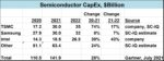
Semiconductor capital expenditures (CapEx) are on track for strong growth in 2021. For many companies the increase should continue into 2022. TSMC, the dominant foundry company, expects to spend $30 billion in CapEx in 2021, a 74% increase from 2020. TSMC announced in March it plans to invest $100 billion over the next three years, primarily for CapEx. Our Semiconductor Intelligence (SC-IQ) estimate is TSMC CapEx will be $35 billion in 2023, but it could go higher.

Samsung is also expected to spend about $30 billion on semiconductor CapEx in 2021. Samsung Group announced a plan to invest 240 trillion won (US$210 billion) over the next three years to expand its businesses. An analyst at Kiwoom Securities in Korea expects about 110 trillion won (US$97 billion) will be semiconductor CapEx. We have estimated Samsung 2022 CapEx at $32 billion, but as with TSMC it could be higher.

Intel surprised analysts in its third quarter 2021 earnings announcement last week with a plan to spend $25 billion to $28 billion on CapEx in 2022, following $18 billion to $19 billion in 2021. Intel will use the funds in an effort to become a major foundry as well as expand and advance capacity for its own products. Based on the mid-point of these ranges, Intel Capex should increase 30% in 2021 and 43% in 2022.

TSMC, Samsung and Intel combined account for over half of total semiconductor industry capital spending. Gartner’s July forecast for 2021 industry CapEx was $141.9 billion, a 28% increase from 2021. Other companies which have projected significant CapEx increases in 2021 include foundries UMC and GlobalFoundries; memory companies Micron Technology and SK Hynix; and integrated device manufacturers (IDMs) STMicroelectronics, Infineon Technologies, and Renesas Electronics.

The semiconductor industry is currently experiencing substantial demand improvement from increased automotive electronic content, 5G smartphones and infrastructure, the internet of things (IoT), data centers, and accelerated PC growth due to pandemic-driven home-based work, education, and entertainment. Gartner’s forecast of 28% CapEx growth in 2021 would be the highest since 29% growth in 2017. Should 2021 CapEx grow 30% or more, it will be the highest since 118% in 2010, 11 years ago.

The big question is how much CapEx is too much? The semiconductor industry has a long history of strong CapEx leading to over-capacity followed by price collapses and a declining semiconductor market. The chart below illustrates the relationship between semiconductor CapEx and the semiconductor market. The green line on the left axis is the annual change in CapEx from 1984 through the forecast for 2021. The blue line on the right axis is the annual change in the semiconductor market. Our analysis at semiconductor intelligence has modeled levels of CapEx change which have a major impact on the semiconductor market. The red Danger line is set at 56%. In years when CapEx growth has exceeded 56%, the semiconductor market in the following year has declined or seen a significant deceleration. The orange Warning line is set at 27%. When CapEx growth has been over 27% but less than 56%, the semiconductor market experienced a decline in the next two to three years.

The table below illustrates this process. There have been six years since 1984 where CapEx growth has exceeded 57%. The most extreme cases were in 1984, 1995 and 2000. In 1984, 106% CapEx growth and 46% semiconductor market growth were followed by a 17% market decline in 1985, a growth deceleration of 63 percentage points. In 1995 Capex grew 75% and the market grew 42%. The next year the market declined 9%, a 50-point deceleration.  In 2000, 82% CapEx growth and 37% semiconductor market growth was followed by a 2001 decline of 32%, a 69-point growth deceleration. In the three other cases (1988, 2004, and 2010) the market did not decline the following year, but growth decelerated by at least 21 points.

Since 1984 there have been two instances where CapEx growth was greater than 27% but less than 56%. In 2006, CapEx growth was 27% and market growth was 9%. Each of the following three years showed decelerating market increases culminating in a 9% decline in 2009. From 2006 to 2009, growth decelerated a total of 18 points. In 2017, CapEx growth was 29% and market growth was 22%. Over the next two years growth decelerated a total of 34 points, with a 12% decline in 2019.

Gartner’s latest forecast is 28% CapEx growth in 2021 and the WSTS forecast is 25% market growth in 2021. Based on the model above, we should see decelerating growth in the next two to three years, with a possible decline in 2023.

While the model shows consistent trends, the rate of CapEx increases is only one factor affecting semiconductor market growth. High CapEx growth years are usually substantial market growth years, as companies use robust current growth as justification for higher CapEx. The vigorous market rise is usually not sustainable, resulting in major growth deceleration or a decline in the following year. End demand changes also are a major factor in semiconductor market declines. In 1985, the emerging PC market had its first decline. In 2001, the internet bubble burst, leading to a collapse in demand for internet infrastructure and other equipment. In 2017, the smartphone market had its first decline, with declines continuing through 2020.

Although substantial CapEx gains can be a predictor of semiconductor market growth deceleration, it is not necessarily cause and effect. However, strong increases in CapEx bear watching in forecasting the semiconductor market.

Also Read:

Auto Semiconductor Shortage Worsens

Electronics Recovery Mixed

Electronics Recovery Mixed


Optical I/O Solutions for Next-Generation Computing Systems

Optical I/O Solutions for Next-Generation Computing Systems
by Tom Simon on 10-28-2021 at 10:00 am

Multiphysics design

According to DARPA the fraction of total power consumed in semiconductors for I/O purposes as been growing rapidly and is creating an I/O power bottleneck. It has reached the point where it needs to be addressed with new technologies and approaches. Interestingly, while the energy density, as measured by pJ/bit for short reach IO – such as chip to chip in the same system – is low, there are so many more connections and higher data volumes that the overall energy required is often higher than in rack to rack connections. Dries Vercruysse, Senior Photonics Design Engineer at Ayer Labs, recently gave a talk at the Ansys Ideas Digital Forum 2021 on how they were motivated to use optical technology for chip to chip communication. He pointed out that the energy efficiency density of longer reach connections has long benefited from the use of optical technology.

There are many hurdles to taking photonics methods for board to board and scaling them so they are effective and efficient enough for use between individual packages. Dries describes how Ayer Labs has developed a solution based on optical modulation using micro-ring resonators.  They have created tunable voltage-controlled resonators that are 1000x smaller than optical devices in traditional ethernet transceivers and are compatible with 300nm CMOS technology. An off-chip laser is coupled from fiber to chip via a vertical grating coupler and then amplitude modulated by varying the bias voltage across the resonator.

Because resonators that operate at different wavelengths can be created by varying physical parameters, one fiber can support many signals in parallel via wavelength division multiplexing (WDM). A single off-chip laser can provide the light source needed for many chips. The Ayer Labs chiplet contains multiple drivers and receivers that then interface externally through short fiber connections to other chips and can be tightly integrated with FPGAs via in-package system-on-chip (SoC).

Dries talked about a Link Demo they performed that connected two chips that each used the Ayer Labs TeraPHY CMOS Optical IO chip. With a remote light source and a bi-directional link, they achieved energy use of <5pJ/bit for both 16Gbps and 25Gbps. The fiber operated at ~5.3 microwatt average power/lambda. During the demo they transferred 104.165 terabits of data without any errors.

Multiphysics Design

Creating this system required extensive simulation of the electrical, physical and optical performance characteristics in their TeraPHY chiplet. For instance, the resonator has semiconductor junctions, optical paths, and even a small thermal heater to help rigidly control the thermal environment. According to Dries this was a perfect example of Multiphysics design. Time frames for each domain were orders of magnitudes apart as well. From picoseconds for the optical, to microseconds for the thermal. They used a wide range of Ansys tools to facilitate their development. The waveguide alone required GPU accelerated IOSMF FDTD simulations with over 1.6 trillion grid points. This was accomplished using the cloud compute environment offered by Ansys.

Ayer labs has already had design success and notable design wins leading to integrations into advanced SoC packages. Dries highlighted their work with Intel FPGAs, including a design that is on a standard PCIe card. Previously, the use of optical fiber was a pipe dream for chip to chip communications. Ayer has shown that it is not only feasible, but it can be effective. The key to their development was having the ability to fully model Multiphysics behavior in a complex environment. The full presentation from the Ansys Ideas Digital Forum 2021 is available for viewing here.

Also Read

Neural Network Growth Requires Unprecedented Semiconductor Scaling

SeaScape: EDA Platform for a Distributed Future

Ansys Talks About HFSS EM Solver Breakthroughs


Memory Consistency Checks at RTL. Innovation in Verification

Memory Consistency Checks at RTL. Innovation in Verification
by Bernard Murphy on 10-28-2021 at 6:00 am

Innovation New

Multicore systems working with shared memory must support a well-defined model for consistency of thread accesses to that memory. There are multiple possible consistency models. Can a design team run memory consistency checks at RTL? Paul Cunningham (GM, Verification at Cadence), Raúl Camposano (Silicon Catalyst, entrepreneur, former Synopsys CTO) and I continue our series on research ideas. As always, feedback welcome.

The Innovation

This month’s pick is RTLCheck: Verifying the Memory Consistency of RTL Designs. The paper was published in the 2017 IEEE/ACM MICRO. The authors are from Princeton and NVIDIA.

Memory consistency is a contract between hardware and software developers on ordering of reads and writes in a multicore system. If two or more threads can load from or store to a logical memory location, given no necessary synchronization between cores and optimizations like out-of-order execution, some orders may be allowed and some may not. There are multiple possible ways to define such rules. An agreed set of rules bounding this behavior defines a memory consistency model (MCM). RTLCheck is the authors’ contribution to automatically check that an RTL design complies with a set of (modified) user-defined axioms encoding an MCM.

The method detects axiom violations as cycles in “happens before” (hb) graphs of test cases, elaborated as fetch-decode/execute-writeback operations across cores. One such litmus test checks message passing between cores. Since arcs in an hb graph denote permitted orderings of operations, a cycle in an hb graph implies a sequence of operations that must complete before they start, which is not possible. The axioms used to prove to an MCM work with abstract architecture specifications. Temporal proof engines used in formal methods for RTL lack this flexibility (per the authors) so axioms are “synthesized” to industry standard System Verilog Assertions (SVA) and constraints with some limitations on what can be mapped.

Paul’s view

Verifying memory consistency in multi-processor (MP) systems is hard, and I’m always a fan of raising abstraction levels as a important way to tackle hard verification problems. The paper’s basic premise to compile high level micro-architecture MCM axioms into SVA is a great idea, and the “happens before” graphs used in these axioms are an elegant and intuitive way to express MCM intent.

The paper is thorough and it’s always nice to see joint research between academia and industry. The authors clearly describe their approach and provide a full worked example on an open-source RISC-V core in which they found a real bug using their methods. Although, as the authors point out, the bug is a bug even for a single instance of the RISC-V core. The memory’s “ready” signal has been accidentally tied to high so the memory is always ready to accept a new value.

I do find myself wondering how much simpler the author’s axiomatic specifications in “Check” tool format are than their synthesized industry standard SVA equivalents. The mapping is 1-1, just more verbose in SVA format. For example, one key observation in the paper is that an SVA for “A implies B happens later” (A |-> ##[1:$] B) can match the case where A happens multiple times before B where an hb-graph axiomatic equivalent would not – imagine that A is “store value x” and B is “load value x”. An intervening “store value y” would obviously invalidate the axiom. Synthesizing additional SVA syntax to prevent multiple A’s before B is one of the paper’s contributions (A |-> ##[0:$]!A ##1 B), but this contribution feels more like syntactic sugaring than a fundamental raising of the abstraction level.

Overall, tight paper, well written, and on an important topic. Also, nice to see the author’s using Cadence’s Jasper formal tool to prove their synthesized SVAs. And find that RISC-V bug 😃

Raúl’s view

For the interested reader, the paper explains axiomatic microarchitectural models in 𝜇spec (first-order logic). Together with the corresponding 𝜇hb (happens-before) graphs and temporal assertions. They walk through a small motivating example with two cores . Each runs a small common “message passing” litmus test of 2 instructions in each core which is easy to follow. The actual generation of the temporal assertions is quite complex and involves additional user non-automatic steps:

  • mapping the litmus test program instructions and values to RTL expressions
  • mapping 𝜇hb graph nodes to Verilog expressions

This requires a “user” with deep knowledge of the field, i.e. axiomatic specifications, 𝜇spec, SVA, RTL, etc. Designers of parallel architectures working with verification experts and access to JasperGold and the check suite [33] can potentially profit from using RTLCheck.

The results are nice: For a 4-core RISC-V, 89% of the generated assertions for 56 litmus tests are completely proven. The remaining 11% complete with bounded proofs. These include the discovery of a real bug in the Multi-V processor and its fix.

As an academic research paper, I find the claims and results stand up, and the concept to be very interesting. However, it is hard to see commercial opportunity in productizing this work. The very high and necessary level of cross-domain expertise and what appears to be a significant level of manual effort does not seem scalable to production applications.

My view

I had hoped this would be a neat lateral way to verify coherency. But Paul and Raúl talked me out of it. The expertise and effort required to setup axioms and constraints to manage formal analysis on a modern SoC seems daunting. I hold out hope that the core concept may still have value. Perhaps when applied (in some manner) in a simulation application.

Also Read

Cadence Reveals Front-to-Back Safety

An ISA-like Accelerator Abstraction. Innovation in Verification

Accelerating Exhaustive and Complete Verification of RISC-V Processors


Intel- Analysts/Investor flub shows disconnect on Intel, Industry & challenges

Intel- Analysts/Investor flub shows disconnect on Intel, Industry & challenges
by Robert Maire on 10-27-2021 at 2:00 pm

Pat Gelsinger Triple Spend

Analysts missed all warning signs until Intel spelled it out
12% stock drop shows disconnect and misunderstanding
No quick fix, this is a long term, uncertain problem & solution
Everyone ignored the obvious until it ran them over

A 12% stock drop is fault of investors/analysts not Intel

Whenever a stock drops 12% in one day there is some sort of major disconnect between the company and the street. Sometimes companies keep bad news under wraps until the quarterly call or just don’t do a good job of “managing expectations” on the street. Sometimes analysts miss not too subtle hints and information until the company spells it out directly.

In the case of Intel’s recent stock drop it is more the fault of analysts and investors missing the obvious rather than the company not communicating. Its also “analysts” not doing some very simple analysis…

Its all about lower margins-more expenses or less revenue or both

It seems that the street completely missed how bad margins would get and for how long. None of this should have been such a surprise as we know Intel’s expenses have and will be going up and that revenues are under pressure from competition and shortages. So it must be the magnitude of those issues that is a surprise

A perfect storm of triple and quadruple spending

We coined a phrase earlier this year about Intel having to “triple spend” that means; 1) spend a lot of money to catch up to TSMC and their technological lead 2) Spend money and margin to have TSMC (their enemy) supply chips for Intel to sell because Intel is lacking in technology and/or capacity 3) Spend money to try to become a foundry player.

We later amended our “triple spend” scenario to “quadruple spend” to account for the spend to acquire GloFo or something like it. Any one of these spend items represents a huge sum of money but taken together it represents a tidal wave of a hemorrhage of money that can hobble even Intel.

More importantly, all four of these new spending sprees is not a one and done, one time spend but rather a long term multi year commitment for each effort.

Missing simple math

Even though the numbers are readily available it seems relatively few people, if anyone, bothered to add and look at the potential sum of spend and the impact it would have on Intel’s expense structure.

Analysts should have able to figure out that capex wasn’t just going to go up 20% year on year and be enough to catch TSMC spending $25B a year, twice Intel. Its clear that Intel has to spend TSMC-like sums of CAPEX and then some more in order to catch TSMC. If we use EUV tool count as a proxy for spend ( which is a good approximation) they need to outspend TSMC now to make up for years of under investment and under buying.

TSMC does not work for free and will not give away its precious leading edge capacity to a company that wants to beat it, without extracting a pound of flesh. TSMC has Intel in a tough position and will squeeze for what its worth and Intel has no choice but to pay up otherwise TSMC will turn on the AMD floodgates.

Becoming a foundry player is not just the $20B to build two fabs in Arizona(let alone fabs in Europe…) and fill them with equipment. Its hiring lots of people (let alone finding the talent) and building the infrastructure (or buying it) needed to service silicon customers. Something Intel wasn’t able to accomplish in the past. Building the two fabs and all associated foundry expenses for something that may not show revenue for years and take a long time to ramp will be a huge drain.

In the meantime renewed competition from AMD (whose product is being built in the same TSMC fabs as Intel) and others as well as emerging competition (like Apple, ARM, Google, Facebook etc…) will negatively impact revenues and pricing. Bottom line is Intel is caught in a longer term margin squeeze.

We were very clear about this and warned investors long ago, before anyone

Way back on March 23rd of this year when Intel announced its foundry intentions we wrote;

Either Intel will have to start printing money or profits will suffer near term

We have been saying that Intel is going to be in a tight financial squeeze as they were going to have reduced gross margins by increasing outsourcing to TSMC while at the same time re-building their manufacturing…essentially having a period of almost double costs (or at least very elevated costs).

The problem just got even worse as Intel is now stuck with “triple spending”. Spending (or gross margins loss) on TSMC, re-building their own fabs and now a third cost of building additional foundry capacity for outside customers.
We don’t see how Intel avoids a financial hit.

Link to original “Foundry Fantasy” note

I don’t think I could have been any clearer, but obviously the message was not received.

Back on January 21st, 10 months ago we said:

Get ready for numbers to look ugly and get sandbagged

Although Intel did not give full years guidance, we would hold onto our seats as we have suggested that the dual costs of increased outsourcing to TSMC added to increased spend on Internal efforts to regain Moore’s Law pace will be high and pressure margins in the short term which we would view as at least the next two years and maybe more.

If Pat is smart he will sandbag strongly and lower expectations to numbers that can be beaten easily and overestimate the costs of fixing 7NM and ramping capacity while still paying TSMC to make chips. He doesn’t want to put out numbers he will miss in his first couple of quarters on the job.

We would hope that this would include a large jump in Capex and R&D to give the engineers and manufacturing the latitude they need.

We were right about the numbers getting ugly but obviously Intel did not “sandbag” enough or manage street expectations enough.

The bottom line is that this margin issue has all been a very long time in the making and should not have been a surprise that cratered the stock. It was all out in the open. If I could figure it out then all the well paid analysts at the large investment banks should have figured it out as well.

Obviously that was not the case as there was a spate of analyst downgrades and shock and surprise that sent the stock tumbling.

The relationship between success and money spent is non linear

One would think that with all the talk about the amount of money (margin) that Intel will be spending that success will be a virtual “lock”. That is far from the case and not reality.

You can throw a lot of money at Moore’s law and still have no guarantee of success. Likewise the foundry business is not a “If we build it, they will come” field of dreams.

Even with all the financial hardship and margin pressure success is not pre-ordained.

This means that we would take statements like all the sacrifice now will be worth it for the future success, with a grain of salt. There is still very high risk in execution as the tasks at hand are huge and complex and its not simply a matter of throwing money at it….but it helps a lot.

The stocks

Even with the 12% drop there is still a lot of risk and a lot of financial pain ahead and we maintain our view that Intel’s stock is better off viewed from the side line. We could see a dead cat bounce or those who feel that there’s a price opportunity but we still see risk and issues for the investable future.

Obviously the semiconductor equipment companies will benefit from increased Intel spend but we already assumed that. Some companies such as ASML will see modest positive impact as they are sold out for 18 months so it matters little to them.

We view the stock action as more of a reality reset rather than any sort of true fundamental change as nothing really changed investors just finally got the memo.

For all those “analysts” who missed the memo we can offer a discount on our newsletter.

Also Read:

LRCX- Good Results Despite Supply Chain “Headwinds”- Is Memory Market OK?

ASML- Speed Limits in an Overheated Market- Supply Chain Kinks- Long Term Intact

Its all about the Transistors- 57 Billion reasons why Apple/TSMC are crushing it


Webinar: A Practical Approach to FinFET Layout Automation That Really Works

Webinar: A Practical Approach to FinFET Layout Automation That Really Works
by Mike Gianfagna on 10-27-2021 at 10:00 am

Webina A Practical Approach to FinFET Layout Automation That Really Works

There are certain tasks that have been the holy grail of EDA for some time. A real silicon compiler – high level language as input and an optimal, correct layout as output is one. Fully automated analog design – objectives as input, optimal circuit as output is another. With the increased layout times, due to the ever-increasing design requirements at advanced process nodes, the automation of advanced node custom layout – high-level commands that implement complex layout tasks with one click, has become another of these holy grails. While I don’t think we’ll see a viable approach for the first two any time soon, I’m here to tell you the third item is indeed available today. Read on to learn about a practical approach to FinFET layout automation that really works.

Background

Pengwei Qian

Dan Nenni was recently joined by Pengwei Qian, the founder and CEO of SkillCAD. You can learn more about Pengwei and his remarkable company in this interview. What followed was a compelling discussion about a new tool from SkillCAD that does address one of the holy grail items, above. There was also a detailed demo to prove it works. The entire event is captured in a webinar. A replay link is coming. First, a bit about SkillCAD, the new product and what you will see in the demo.

SkillCAD was founded in 2007 to enhance the productivity of Cadence Virtuoso by providing capabilities not offered by the Virtuoso environment. Today, over 85 companies use SkillCAD. The webinar details a new product from SkillCAD – IC Layout Automation Suite (LAS) Advanced. This product is focused on advanced node layout for TSMC, N7 down to N3.

Pengwei explained that there is an exponential increase in design rule complexity at these nodes, making it impossible to maintain consistent layout designer productivity. He explained that SkillCAD addresses this problem.

IC LAS is a collection of over 120 user-guided layout and auto-routing commands. Highly complex operations are reduced to one mouse click and productivity improvements in the 30% – 50% range have been observed.

The Demo

What followed was a live demo of the new tools. The examples shown all ran in real time. This is very impressive to watch once you understand the complexity of what is being automated. You need to watch the demo to really get the full impact. Here is just a summary of the functions demonstrated by Pengwei:

  • Auto connect all items on a net with one click using the Dot Connector command. All wiring and vias are created, obeying the large set of process design rules. You can also specify the order of connection in a dialog box and again, with one click the connections will be implemented. The user can also move wiring around, again with one click. Horizontal and vertical connections can be done this way.
  • Auto connect specific nets with a couple of clicks using the Line Connector. The number of necessary clicks doesn’t increase with the number of lines you are connecting. So, the same two clicks can connect two, twenty, fifty, or more lines on the same net. 
  • Support for Cadence or user-defined coloring methodologies with the Quick Color command. Coloring methodologies can be easily specific by click, by line (draw a line through nets and specify color rules), by WSP (width spacing patterns) to apply coloring rules to all wires in a WSP and finally using the Search function to find metal that isn’t colored.

To Learn More

Pengwei then explained where to find additional details on the tool and its capabilities on the SkillCAD website.  A very impressive and informative event. The webinar concludes with a very relevant and useful Q&A session. If you are involved in layout at advanced nodes, you need to watch this webinar. You can access the replay here.   A practical approach to FinFET layout automation that really works, is now available.

Also Read:

WEBINAR: SkillCAD now supports advanced nodes!

Webinar: Increase Layout Team Productivity with SkillCAD

SkillCAD Adds Powerful Editing Commands to Virtuoso


Cadence Reveals Front-to-Back Safety

Cadence Reveals Front-to-Back Safety
by Bernard Murphy on 10-27-2021 at 6:00 am

J897 Functional Safety Press Image small min

This is another level-up story, a direction I am finding increasingly appealing. This is when a critical supplier in the electronics value chain moves beyond islands of design automation to provide an integrated solution for the front-to-back design for capabilities now essential for automotive and industrial automation clients. For whom safety must run through all the design process. In coverage, adding safety coverage. Integrating digital and analog fault campaigns. In automated safety mechanism insertion and verification. In optimizing verification engines (digital and analog) for maximum parallelism and throughput. Intelligent fault list reduction. And, in some ways most important, in providing an accessible status portal for safety managers to view design-for-safety status without need for EDA tool expertise.

Why is a front-to-back solution important?

The boom in ADAS and safety features isn’t simply because ADAS features are cool and safety is generally a good thing. The European New Car Assessment Program (Euro NCAP) has been tracking new car introductions on several fatality metrics, for adult and child occupants for example, rating cars on a 5-star system against several safety tests. These ratings are generally available and have had a startling positive impact on road fatalities over a decade or more. Auto makers are putting heavy emphasis on further advanced ADAS features since these ratings are directly affecting the saleability of their products.

Those needs then ripple down the supply chain, increasing emphasis on higher ASIL certifications and fail-operational implementations. The latter require safety islands to monitor in-operation integrity and ability to isolate out-of-spec circuitry. Which increases need in design to explore tradeoffs in safety mitigation techniques, to have robust safety planning and analysis, very effective and efficient fault campaign support across digital and analog circuitry and the means to roll all that back up to the top level FMEDA plan. These needs, together with early customer feedback, have guided Cadence’s development of their safety solution.

The solution architecture

Frank Schirrmeister (Senior Group Director, Solutions at Cadence) told me how to think of this. As a technology horizontal (safety in this case) across vertical markets. This horizontal integrates across three of the five Cadence domains: digital and analog implementation, and verification, with an intent to get to faster safety certification for automotive and industrial designs.

At the top level is a new tool, the Midas Safety Platform, driving management of the FMEDA campaign and providing a unified interface to all underlying Cadence engines. Primary users of this platform would probably be architects, safety managers and product managers. People who don’t want to get into the details of understanding and running those underlying tools but who do want to be able to extract useful information. To experiment with options and assess current safety status. The tool runs on both Windows and Linux for this reason. It manages internally the complexity of gathering such data from the domain tools. Midas also supports USF, a Unified Safety Format to exchange and manipulate safety information across different Cadence tools.

The digital safety design platform incorporates multiple improvements in support of this release. vManager now has  safety-centric capabilities. Xcelium has been further optimized for serial and concurrent fault simulation. Xcelium-ML is also fault simulation-aware to reduce regression run-times. Implementation choices for safety mitigation, user-specified from the top, are implemented through Genus synthesis and validated through Conformal equivalence checking.

The analog/AMS functional safety flow has been developed in alignment with the IEEE P2427 proposed standard. The flow integrates Spectre for simulation and Legato for reliability, adding a new fault assistant for rule-based fault identification. The solution automates launching fault simulations for different failure modes. It also accelerates functional safety closure by annotating safety diagnostics back to Midas.

Customer validation

Cadence has been working with multiple customers to validate and refine this solution and have several public endorsements. The Arm automotive and IoT line of business has endorsed the solution. Hailo, a well-respected AI at the edge company and Melexis, a European manufacturer of semiconductor products, both used in automotive designs ,are on board. And ST, widely known for industrial solutions and sensing expertise has provided endorsement. Pretty solid backing.

You can learn more about the Cadence Safety Solution HERE.

Also Read

An ISA-like Accelerator Abstraction. Innovation in Verification

Accelerating Exhaustive and Complete Verification of RISC-V Processors

Side Channel Analysis at RTL. Innovation in Verification