Synopsys 800x100 px High Quality

Webinar – How to manage IP-XACT complexity in conjunction with RTL implementation flow

Webinar – How to manage IP-XACT complexity in conjunction with RTL implementation flow
by Daniel Payne on 10-26-2021 at 10:00 am

RTL Integration

Standards help our EDA and IP industry grow more quickly and with less CAD integration efforts, and IP-XACT is another one of those Accellera standards (1685-2009) that is coming of age, and enabling IP reuse for SoC design teams. Here at SemiWik, we’ve been writing about Defacto Technologies and their prominent use of IP-XACT since 2016. I just learned about a new webinar from Defacto, planned for November 10th at 10:00AM PST.

Challenges

With any complex standard it can take awhile to develop an efficient methodology for SoC design, and it’s expected that in 2021 we’ll see a new standard version emerge. Having compliance with an RTL implementation flow can be rather painful and not obvious for first-time designers.

Webinar Overview

Today, an increased number of IPs are delivered using IP-XACT interfaces which should ease the integration process. However, it is still a complex format to handle and not every company (or designer) wants to jump into a new format. The tight relationship between the standard and RTL will be highlighted in the webinar, along with using more automation to keep them correlated. Both system level and RTL designers are going to benefit from attending the webinar.

We observe several categories of users and reactions around IP-XACT:

  • Those who are already using IP-XACT but would like to have the design information fully compliant with an RTL design flow
  • Those who want to adopt this standard with full compliance with RTL design flow but are a bit reluctant knowing the format complexity.
  • Those who want to avoid using IP-XACT as much as possible

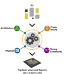
Defacto’s SoC Compiler addresses users above and helps building a unified and IP-XACT and RTL design flow. During this webinar Defacto’s SoC Compiler 9.0 key capabilities will be illustrated through typical cases such as:

  • Extraction of design information
  • Coherency checks between IP-XACT, RTL, UPF and SDC
  • IP-XACT <-> RTL view generation
  • Joint IP-XACT & RTL Integration
  • System level handling and report with a focus on memory map.

SoC Compiler

SoC Compiler provides unique capabilities to build a complete SoC at RTL with all the mechanisms to edit the design and deliver a correct-by-construction RTL and the associated views such as SDC and UPF, ready for synthesis.

RTL Integration

SoC Compiler enables the SoC design assembly process with full support of IP-XACT standard in full compliance with RTL files. Several automated design “extraction, packaging and reuse” capabilities are provided. Defacto is part of the Accellera committee for the definition of IP-XACT standard and an active member of the IP-XACT 2021 version

SoC Compiler

Summary

During the webinar, attendees will get a clear picture of how SoC Compiler helps to build a cost-effective and robust flow to manager IP-XACT complexity. Register for the REPLAY here.

About Defacto Technologies

Defacto Technologies is a leading provider of RTL design solutions which help users to build a unified design flow where different standards like RTL, IP-XACT, UPF for power intent, SDC for timing constraints, LEF/DEF for physical design information, are considered. Defacto SoC Compiler is a silicon proven EDA solution which are helping major semiconductor companies to add automation to their design flows mainly at RTL and enhance integration, verification and Signoff of IP cores and System on Chips.

Related Blogs


Physically Aware SoC Assembly

Physically Aware SoC Assembly
by Bernard Murphy on 10-26-2021 at 6:00 am

SoC Assembly min 1

We used to be comfortable with the idea that the worlds of logical design and physical implementation could be largely separated. Toss the logical design over the wall, and the synthesis and P&R teams would take care of the rest. That idea took a bit of a hit when we realized that synthesis had to become physically aware. The synthesis tool vendors stepped up and can now optimize to floorplan constraints. Problem solved? Not quite. Now we need physically aware SoC assembly as physical constraints are intruding into SoC design.

Power management constraints

A widely recognized reason for this shift is due to power and voltage islands. These need to be driven by appropriate power buses, connecting to voltage regulators or external power sources. This is a very physical constraint. So what? You decide what blocks need to go in what domains and pass that information to the implementation team. They’ll take care of the floorplan and power buses. But here’s the problem. Modern SoCs may need hundreds of these domains, which evolve and shift as the design evolves, and as power optimization is refined.

Power buses must be consolidated between domains with common power requirements to minimize area and congestion overhead that comes with these buses and regulators. This also implies that functions consolidated under common buses must be close together in the floorplan. Which ripples through into gathering functions within a group into an additional level of hierarchy to simplify life for the UPF development team, the verification team and the implementation team. Then again, maybe some sub-function of an IP needs to be in a different domain than the rest of the IP, so you must restructure that part into a different group. These changes are not one-time decisions. Hierarchy optimizations for power can remain somewhat fluid until you know you are meeting your power goals. Sometimes quite late in the design schedule.

Subsystem reuse

We often think of reuse in terms of IPs. Commercially supplied blocks or proven in-house functions. However, reuse is just as important, maybe more important, for pre-designed subsystems, though usually not as an exact reuse. Some changes you may need to make here are again driven by power management choices. Maybe the hierarchy choices you made for a previous design aren’t quite right for a derivative and need to be tweaked. Some functions that were in an always-on domain need to move into a switched domain, and some switched functions now need to be always-on.

Sometimes the need for moving functions around in the hierarchy isn’t motivated by power. Think of a memory subsystem, for example. Designed, debugged and field-proven in your first product release. You want to use the same subsystem in a derivative product. But the way this is going to floorplan, the DDR PHY is going to be facing into the design, not towards the die edge. Again, you’d like to do some restructuring to simplify moving this around in implementation.

Restructuring assembly

RTL is very powerful, but one area it really fails is flexibility in design hierarchy. Once you have defined a hierarchy, it becomes very difficult to change. For simple changes, you might consider scripting, but that approach quickly runs out of gas. Try moving two instances out of a block into a different block at the same level. You will need to rubber-band some connections back into the original block, possibly through new ports. Or be able to replace some by direct connections in the second block. Then you’d need to remove redundant ports  on both blocks. And so on.

The complexity of moving functions around in a hierarchy quickly becomes apparent. Script-based approaches are simply too difficult. SystemVerilog or VHDL syntax compound the problem further. These are transformations that require serious EDA know-how and validation across multiple customers. You still should run equivalence checking between the before and after netlists to double-check. But you want that to be a confirmation, not a step in an endless cycle of corrections.

The Arteris IP SoC/Hardware-Software Interface (HSI) development product provides automated support for this restructuring in SoC assembly. Proven on many designs. Make these complex transformations a differentiated opportunity for your product team, not a roadblock.

Also Read:

More Tales from the NoC Trenches

Smoothing the Path to NoC Adoption

The Zen of Auto Safety – a Path to Enlightenment


The Challenge of Working with EUV Doses

The Challenge of Working with EUV Doses
by Fred Chen on 10-25-2021 at 2:00 pm

The Challenge of Working with EUV Doses

Recently, a patent application from TSMC [1] revealed target EUV doses used in the range of 30-45 mJ/cm2. However, it was also acknowledged in the same application that such doses were too low to prevent defects and roughness. Recent studies [2,3] have shown that by considering photon density along with blur, the associated shot noise could easily account for such defects and roughness. Given that the blur is on the order of 5 nm, we can easily estimate the suitable photon density, by taking 3 standard deviations as 10% of the nominal dose. This gives 3*sqrt(N)/N = 10%, or N = 900 photons, which are distributed, on average, over a 5 nm x 5 nm estimated blur area, giving 36 photons/nm2, or 53 mJ/cm2. Such a dose may be considered too high for satisfactory throughput, based on the throughput-dose curve below [4]:

Figure 1. Throughtput vs. dose for NXE:3400C EUV tool with 300W source [4].

Going from the usually specified 30 mJ/cm2 dose to 53 mJ/cm2 reduces the throughput from 140 to 100 WPH. If we consider not incident EUV dose, but actually absorbed EUV dose, to reach the 53 mJ/cm2 target, it gets even worse. A metal-organic resist (MOR) could absorb 55% of the dose, which would bring the required incident dose to 96 mJ/cm2, which means a throughput of around 75 WPH. A conventional chemically amplified resist (CAR) on the other hand, absorbs around 20% of the dose, leading to a required 265 mJ/cm2, which means around 30 WPH.

Not surprisingly, EUV users would want to find a way to stay below 50 mJ/cm2. The proposed approach described in US20210096473 [1] uses directional etching. The etch tool is modified to produce directed etching ion beams along one axis, so that etching only proceeds significantly along that axis and negligibly along the other axis. Note that normally, etching would be negligible along both axes. Presumably, such vertical etching would preserve pre-existing roughness. The obvious drawbacks of this directional etching approach are: (1) it’s limited to unidirectional features, and (2) line ends are hard to control.

A more accurate picture of EUV doses would require consideration of photoelectrons and secondary electrons, which would require intense calculations beyond the simple estimates here.

References

[1] R-G. Liu et al., US20210096473, assigned to TSMC.

[2] https://www.linkedin.com/pulse/stochastic-behavior-optical-images-impact-resolution-frederick-chen

[3] https://www.linkedin.com/pulse/blur-wavelength-determines-resolution-advanced-nodes-frederick-chen

[4] J. van Schoot et al., Proc. SPIE 11517, 1151712 (2021).

Related Lithography Posts


Verification Completion: When is Enough Enough?  Part II

Verification Completion: When is Enough Enough?  Part II
by Dusica Glisic on 10-25-2021 at 10:00 am

Tunnel min

Verification is a complex task that takes the majority of time and effort in chip design. At Veriest, as an ASIC services company, we have the opportunity to work on multiple projects and methodologies, interfacing with different experts.

In this “Verification Talks” series of articles, we aim to leverage this unique position to analyze various approaches to common verification challenges, and to contribute to make the verification process more efficient.

The first part of my discussion with experts in the field is presented in the previous article. It deals with the way in which the criteria for completion are formed and what exactly those criteria are. The experts I talked with were Mirella Negro from STMicroelectronics in Italy, Mike Thompson from the OpenHW Group in the Canada and Elihai Maicas from NVIDIA in Israel.

Tracking the development process

Of course, everyone uses tools from well-known vendors (Synopsys Verdi or Cadence vManager) since unfortunately, as Mike notes, “there is a general lack of open-source tools for generating and collecting usable verification quality metrics.”

On top of this, Elihai uses locally developed tools and scripts to send automated reports in the e-mails. “It’s convenient if all the criteria are formalized to a number that can be collected like coverage percentage. For flows/features, I usually also add coverage item (SVA or just test-pass hit). This way it is visible in all the automatic reports,” he explains.

Mike is a big fan of verification plans and uses their items to track the progress. This is how the process looks like for him: firstly, write and review a detailed verification plan, then assign a qualitative metric to each item in the plan (a cover point, a testcase, an assertion or code coverage) and afterwards develop tests and run regressions until your metrics show that all items in the verification plan are covered.

Mirella, on the other hand, relies a lot on the members of her teams and trusts their assessments and reports related to the planning, as well as to the monitoring of progress. They have crafted a spreadsheet that is simple for engineers to fill out although it has some complex formulas behind it. Each team member reports his own progress using this form. And, as a manager, Mirella uses a business data intelligence tool to analyze all these spreadsheets, which gives her a clear overview of the status. It can give a nice graphical representation of the status of tasks, resources or whatever needed.

Major causes of oversights and problems

So, what can go wrong? Mike believes that “the bulk of the complexity in ASIC verification is simply dealing with the extremely large number of features to cover.  It is all too easy to miss an important detail.  A big source of this can be insufficient information in either a specification or verification plan.  Another significant source of test escapes comes from a lack of time and engineering resources.  There will never be enough time and never be enough people, so it’s important to prioritize the items in your verification plan. Some features simply must work, or the project fails. These should be done as early as possible.”

Elihai says that major pitfalls may occur when not documented well in three situations: specs are changed during the development, new information generated during design review meetings and decision made by architect and designer and not communicated to the verification team.

In Mirella’s view, the major problems are caused by lack of the time which comes from bad planning and “invisible tasks” (sick leave, trainings, holidays, assisting a colleague, meetings…). She overcomes this issue by calculating in the plans that an engineer has less than five working days a week. Also how effectively they work depends on the seniority level. Mirella also adds a risk margin which is usually 10% of the project duration, but it can vary based on the risk analysis.

Finally, how do you cope with the anxiety that comes with “pressing the signoff button”?

According to Elihai, he never finishes all his plans for verification. But he tries to find out what are the things that must be verified, such as important flows or end-to-end data transactions. He regularly maintains a tasks list and constantly prioritizes them with relevant stakeholders (architects, designers, managers). Besides some strict rules, this process also has some “intangible” factor that comes from experience and intuition. And then you just have to trust what you did was enough.

Luckily, from Mike’s experience it usually is: “Create a plan, follow the plan, track progress according to the plan.  When the device is taped out, you’ll know what you’ve verified and how well it’s verified. Any time I have done this, the results have been positive.”

But he still admits:” Having said that, it’s always stressful.”

Takeaways

So, to make a sign-off less stressful, we need to do detailed planning, follow that plan, have well-organized communication between all relevant stakeholders, establish a trust within the team, but also not to be afraid to follow the intuition in some situations.

To view more about Veriest, please visit our web site.

Also Read:

Verification Completion: When is enough enough?  Part I

On Standards and Open-Sourcing. Verification Talks

Agile and DevOps for Hardware. Keynotes at DVCon Europe


Design Planning and Optimization for 3D and 2.5D Packaging

Design Planning and Optimization for 3D and 2.5D Packaging
by Tom Dillinger on 10-25-2021 at 6:00 am

platform

Introduction

Frequent SemiWiki readers are aware of the growing significance of heterogeneous multi-die packaging technologies, offering a unique opportunity to optimize system-level architectures and implementations. The system performance, power dissipation, and area/volume (PPA/V) characteristics of a multi-die package integration are vastly improved over board-level designs with discrete parts.

The ability to select different technologies for various system functions (as “chiplets”) in the composite 2.5D/3D package adds the dimension of overall product cost to the PPA/V optimization parameters. System development costs are addressed by the potential to leverage chiplet reuse. Production cost assessments address the tradeoff between the additional complexity of 2.5D/3D package design/assembly versus the yield impact of integrating functionality into a single larger die. This tradeoff is influenced strongly if the PPA goals of architectural blocks can be achieved with existing chiplets in older process technologies.

Given these opportunities for system optimization, the diversity of 2.5D implementations (with area >>1X the maximum reticle size) will continue to grow. Similarly, the complexity of 3D stacked die topologies will also increase, with connectivity between the die transitioning from using microbumps to a bumpless, thermo-compression bonded connection between die pads and through-silicon vias (TSVs).

With the emergence of these system-level implementations, there has been a corresponding focus on the requisite EDA flows to support the design planning and configuration management steps. Initially, the 2.5D/3D product teams incorporated a mix of traditional package and SoC implementation tools, passing connectivity and physical models back and forth. The partitioning of the system architecture into chiplets was somewhat ad hoc, often requiring multiple iterations between disparate tools to achieve a routable solution.

The increasing demand for chiplet interface bandwidth and the complexity of the (“short reach”) chiplet interface timing meant that corresponding timing and signal integrity analysis steps need to be an integral part of the initial design process. The higher power dissipation density associated with 3D die configurations also requires thermal analysis to be an early design convergence evaluation.

In short, the growing importance of architectures pursuing 2.5D/3D package implementations necessitates a unified EDA platform, spanning the tasks of system planning to preliminary electrothermal analysis closure.

Cadence Integrity 3D-IC Platform

To address the needs of advanced package design, Cadence recently announced their Integrity 3D-IC platform. I had the opportunity to chat briefly with Vinay Patwardhan, product management group director in the Digital & Signoff Group, about the development and key features of the platform.

The figure below provides an overview of the platform functionality.

Vinay indicated, “The heart of the Integrity 3D-IC platform is the unified database. The sheer data volume associated with a 3D system design, combined with the tools needed for physical implementation and design rule verification, meant building the Integrity database from IC-based roots. The Cadence Innovus data model served as the foundation, with specific enhancements for Integrity 3D-IC.”

Vinay highlighted the following database features:

  • Representation of the partitioned 2.5D/3D model hierarchy
  • Support for multiple technology files for the heterogeneous process models for various chiplets
  • Integrated version and configuration management to support the system architecture decomposition and optimization
  • Maintaining cross-correlation links between physical, timing, and electrical data for pins/nets, pads/bumps, TSVs, and chiplet models

With regards to chiplet models, I asked Vinay about the integration of existing chiplet IP into the system design. He replied, “The Integrity 3D-IC database supports multiple views for a node in the design hierarchy. There are interfaces to import/export standard netlists and model formats, such as Verilog, DEF, LEF, SDCs, boundary model formats like ILM timing abstracts and OpenAccess physical boundary data. Special formats in which package layouts are represented can be read in seamlessly as well.” (More details about the Integrity 3D-IC database are provided in a Cadence white paper. Please refer to the link at the bottom of this article.)

As mentioned above, the confidence in the 3D implementation requires a platform that enables timing, electrical, and thermal analyses to be pursued during the initial system partitioning phase. The figure below depicts the Integrity 3D-IC system-level flow manager, with the corresponding Cadence tool interfaces.

Yet, how do the system architect and packaging engineering teams get started? How can they quickly iterate on early partitioning activities, confident that the bump/pad planning and inter-chiplet connectivity will be realizable before pursuing the analysis flows?

Vinay highlighted a specific feature of the Integrity 3D-IC platform.  The system planner GUI is illustrated below, depicting the system architecture in multiple physical and connectivity views.

Vinay delved into a key innovation in Cadence’s Tempus Static Timing Analysis (STA) that can be called through the Integrity 3D-IC platform. Specifically, with many discrete heterogeneous die incorporated into the package, the potential number of timing analysis “corners” multiplies quickly, potentially in the thousands. The figure below highlights the issue along with the technology developed to address this specific challenge.

Vinay said, “The Tempus STA tool supports boundary models in conjunction with concurrent, multi-mode, multi-corner (C-MMMC) analysis for data reduction and to simplify job management. On top of that, we have added a special feature called rapid, automated inter-die (RAID) analysis, which is a ‘smart pruning’ feature to reduce the number of analysis corners designers need to consider when performing 3D timing analysis in Integrity 3D-IC.”

I asked about the availability of Integrity 3D-IC. Vinay replied, “We have multiple customers who have helped with the evolution of the platform and are using it now.” (The Cadence press release includes several reference testimonials – see the link below.) Vinay added, “And, we are closely engaged with all the leading silicon foundries and advanced packaging technology providers.”

Summary

The growing adoption of 2.5D/3D package technologies offers unique “More than Moore” opportunities for PPA/V and cost-optimized system implementations. Early 2.5D/3D designs used disjoint tool flows, within limited system planning exploration options. A unified platform, flow manager and model database are needed to provide users with the ability to manage heterogeneous chiplets and enable analysis flows to be a fundamental part of the initial system partitioning. The recently announced Cadence Integrity 3D-IC platform addresses those requirements.

For additional information, please follow the links below.

Cadence Integrity 3D-IC home page

Cadence Integrity 3D-IC press release

Cadence Integrity 3D-IC white paper

-chipguy


LRCX- Good Results Despite Supply Chain “Headwinds”- Is Memory Market OK?

LRCX- Good Results Despite Supply Chain “Headwinds”- Is Memory Market OK?
by Robert Maire on 10-24-2021 at 10:00 am

Lam Research Report 2021 SemiWiki

Lam- good quarter but supply chain headwinds limit upside
Memory seems OK for now but watch pricing
China will also weaken which may add caution
Performance remains solid as does technology prowess

The yellow caution flag in the Semi race impacts Lam as well

As we suggested two weeks ago and saw with ASML this morning, supply chain issues are coming home to the semiconductor industry itself. While not yet putting a major dent in business we are seeing some weakness or caution in outlook.

Despite all this, Lam put up great numbers. Revenues at $4.3B were a tad on the light side but still resulted in good earnings at $8.36/share. Street numbers were $4.32B and EPS of $8.21. Guidance is for $4.4B +-$250M and EPS of $8.45 +- $0.50 versus street of $4.4B and $8.47…so more or less in line. A half beat and an “in-line”.

Lam remains the “poster child” for memory sector

Memory was 64% of Lams business with NAND being about 70% of that. Although Lam management went to ;lengths to talk about foundry/logic they are still inextricably tied to memory as their mainstay.

Memory pricing weakness could be an early negative sign

We have started to see some weakness in memory pricing with the weakness already reaching some retail products in the form of discounted pricing on SSD’s.

We are likely at or past the peak demand season for memory on a seasonal basis. Much memory related product bound for holiday sales is already built and on a boat to the US.

The memory industry usually sees its weakest period in the post holiday period of Q1.

Memory has not been the cause of most of the reported semiconductor shortages and has remained in good supply.

We need to continue focus on the memory space as memory makers are usually the fastest at shutting off the spigots of new capacity and tool buying in the chip industry as they tend to have the fastest reaction and shortest outlook radar. While ASML has an 18 month backlog, Lam is more of a turns business.

Supply Chain headwinds are less complex

While Lam talks about supply chain headwinds like shipping costs and issues we do not think they are nearly as complex as ASML which makes a much more complex tool with a much more complex and international supply chain.
Lam also spoke about some margin pressure due to the start up ,of its new Asian manufacturing whose costs are not yet amortized.

Lam still says it is supply constrained and it does not appear that the constraint is going away and it obviously is weighing down the future outlook.

Despite the caution business is at record levels- Imagine a Duck

Despite all the concerns business is at record levels. We may be seeing a bit of slowing as you can’t grow that fast forever but its still great.

Shareholder returns and financials are all in fantastic shape. We imagine the image of a duck everything appears calm and beautiful on the surface but likely furiously paddling away underneath the water to make shipments and get components.

The stock

Given the conservative outlook coupled with the softness of revenues, investors are not going to be happy. Add to that some concerns about supply chain headwinds and a sprinkling of memory nervousness and you will see stock weakness.

As with others in the sector it appears that the stocks may have rolled over with no real catalyst to get them moving again.

The dreaded “supply chain” words have gone from a positive influence of chip shortages to a negative influence of sand in the gears of production. While the numbers are still great the “spin” is not at all positive.

It would be nice to be able to bottle up all the great results to save them for a time when they would be more of a positive influence on investors but alas that is not the case.

Also Read:

ASML- Speed Limits in an Overheated Market- Supply Chain Kinks- Long Term Intact

Its all about the Transistors- 57 Billion reasons why Apple/TSMC are crushing it

Semiconductors – Limiting Factors; Supply Chain & Talent- Will Limit Stock Upside


ASML- Speed Limits in an Overheated Market- Supply Chain Kinks- Long Term Intact

ASML- Speed Limits in an Overheated Market- Supply Chain Kinks- Long Term Intact
by Robert Maire on 10-24-2021 at 6:00 am

ASML Report 2021

ASML great QTR but supply chain will limit acceleration
Products are most complex with most extensive supply chain
Long term position fantastic but investors will be nervous
300M pushouts in DUV with EUV still on track

Good quarter but yellow caution flag is out for supply chain concerns

ASML reported great revenues of Euro5.2B and EPS of Euro4.27 per share. Most importantly the order book was Euro6.2B with Euro2.9B of EUV bookings.

It was reported on the call that roughly $300M of DUV sales slipped due to supply chain issues combined with issues with ASML’s new logistics center. Revenue was a slight miss versus street expectations while earnings exceeded expectations.

The bigger question is going forward expectations which may have to come down based on supply chain constraints. EUV expectations for 2022 appear steady at 55 units with the orders for EUV tools booked up into 2023. DUV expectations may be more of an issue going forward.

We warned investors of supply chain issues in Q3 & beyond 2 weeks ago

We had been hearing more and more about strains in the supply chain for semiconductor equipment tools and materials. On Oct 4th we put out a newsletter in which we warned of risk to the semi stocks based on these supply issues;

Semiconductors- Limiting factors; supply chain & talent -Will limit stock upside

We specifically mentioned ASML as one of the risks in the supply chain itself. The semiconductor supply chain is by far the most global and most complex and thus the most exposed to disruptions.

ASML tools make the moonshot look easy

We have mentioned many times about the fantastic complexity of ASML tools especially EUV which has taken literally over 30 years of global effort to bring about. The supply chain is very long and far reaching across the globe.

Some components such as the lenses have a very finite supply that is very difficult and time consuming to expand upon.

At one point, back a while ago, one of the limiting factors was not enough young Germans wanted apprentice for many years to learn how to polish the glass used in the lenses. Obviously much of that has been automated but limits still exist due to the highly specialized nature.

ASML stated on the call that they had eaten into their “safety stock” (kind of like strategic reserves) of DUV components and the cupboard was now bare. Basically we have stretched the supply chain to the point where we just can’t easily get anymore out of it. Any flexibility of supply is fading.

This underscores our warning of two weeks ago that the upside from here will be more limited as we asymptotically reach an upper bound of growth in the near term.

What if its not just a near term limit or plateau but a cyclical peak?

While it certainly feels like a near term constraint it could also be a cyclical peak. The stocks certainly seem to be behaving as if its a cyclical peak that we are bouncing off of.

The question circles back around to how bad the hangover will be after he current party is over… Do we way overshoot and build so much excess capacity into the industry that prices collapse for years?

Do we slowly slow down into a soft landing where capacity finally catches up with demand that continues to grow at an accelerating pace? Its still too early to tell but investors will be very, very nervous that they have seen the cyclical movie before and it never ends well.

EUV remains very solid

On the plus side, demand and orders for EUV tools as well as production seem somewhat largely unaffected, which is all important as the ASML story is all about EUV. We see no reason to expect any change in EUV demand for the foreseeable future as Moore’s Law demands the shift to EUV.

DUV demand likely exceeded previous plans as in a “normal” semiconductor industry with litho steps moving to a new technology you are usually less inclined to go out and buy more tools of the older technology as the mix is declining.

Obviously the unexpected demand for older semiconductor capacity turned the normal Moore’s Law flow and strategy on its head, hence the bigger than planned demand for DUV tools which ASML wasn’t counting on.

Still a monopoly with great financials

We have to remember not to lose sight of the reality that ASML remains a virtual monopoly in a fast growing industry with technology on its side.
The fundamentals have nor changed at all, just some relatively insignificant timing due primarily than higher than expected growth. Its a very high class problem to have, more growth than you can satisfy.

I am getting tired of two words “supply chain”

The buzz words of the month are clearly “supply chain”. These two words have supplanted many other words in the nightly newscast. Next I am sure that QAnon will take up some wild theory about a supply chain conspiracy to take down the global economy…film at 11.

Yes, indeed, the supply chain has impacted many industries and the catalyst of “supply chain” issues started with Covid but was clearly brewing for a very long time.

There are many supply chains; food, energy, pharmaceuticals, all of which have become overly complex, global and therefore vulnerable.

While its clearly not good to take an isolationist view, like the hermit kingdom, there certainly needs to be an awareness and planning for the exposure

The stocks

Obviously ASML has gotten whacked as it is no longer a “perfect” story. While other semiconductor equipment makers do not have as complex a supply chain they nonetheless remain exposed to potential disruptions.

ASML’s stock was priced for perfection and we had warned that anything less than perfect performance would cause a sell off and that’s what we have seen.
We would expect similar reactions to any other stock that reports weakness or exposure. We also think the the probability of such an event is increasing as supply chains get stretched further.

Other companies have more diverse product lines that may be able to absorb shortages in one area with strong demand in other areas.

As collateral impact from ASML we would point to semiconductor companies that won’t be able to ramp expansion as quickly as expected. We have gone into detail previously on the risks to companies like Intel and their need for ASML tools.

ASML is the key to Intel’s resurrection

ASML also pointed out that they and other equipment makers need to get semiconductors in order to build more tools to make more semiconductors. Right now these seem more like inconveniences than major problems.

While its less likely that the long term positive trend will be impacted, we think that the stocks, which are always more skittish, will continue to be soft as investors get more nervous and risk averse until we stop hearing “supply chain” in the nightly news.

Clearly the news flow slowed down about semiconductor shortages (which was a positive for chip stocks) while the news about supply chain has turned into a negative for chip stocks.

Also Read:

Its all about the Transistors- 57 Billion reasons why Apple/TSMC are crushing it

Semiconductors – Limiting Factors; Supply Chain & Talent- Will Limit Stock Upside

ASML is the key to Intel’s Resurrection Just like ASML helped TSMC beat Intel


Podcast EP44: Open Hardware Diversity Alliance

Podcast EP44: Open Hardware Diversity Alliance
by Daniel Nenni on 10-22-2021 at 10:00 am

Dan and Mike are joined by Kim McMahon, Director of Visibility & Community Engagement, RISC-V International and Rob Mains Executive Director, CHIPS Alliance. Kim and Rob are working with individuals and companies to promote diversity and inclusion in the open hardware industry. We explore their strategies, goals and plans to increase participation by women and under-represented individuals in the open source community.

https://riscv.org/

https://chipsalliance.org/

The views, thoughts, and opinions expressed in these podcasts belong solely to the speaker, and not to the speaker’s employer, organization, committee or any other group or individual.


CEO Interview: Jothy Rosenberg of Dover Microsystems

CEO Interview: Jothy Rosenberg of Dover Microsystems
by Daniel Nenni on 10-22-2021 at 6:00 am

Jothy Rosenberg 1

Jothy Rosenberg is a serial entrepreneur, founding nine different startups since 1988, two of which sold for over $100M. Currently, he’s the Founder & CEO of Dover Microsystems, the first oversight system company. Earlier in his career, Jothy ran Borland’s Languages division where he managed languages like Delphi, C++, and JBuilder. He earned his BA in Mathematics from Kalamazoo College and his Ph.D. in Computer Science from Duke University (where he started his career as a professor of Computer Science).

Jothy has written three technical books, but his pride and joy is his memoir, Who Says I Can’t; it tells his inspiring story of using extreme sports to regain self-esteem after losing one of his legs and a lung to cancer, as a teenager. Bearing the same name as his memoir, Jothy founded and runs The Who Says I Can’t Foundation, a non-profit organization with a mission to help disabled individuals get back into sports. He also created and hosted the Who Says I Can’t TV series on YouTube and is TEDx speaker.

What’s the backstory behind Dover Microsystems?

While Dover Microsystems may have been founded in 2017, the core components of our CoreGuard® technology have been in development since 2010. CoreGuard started as a DARPA CRASH program proposal, submitted by Dover’s Chief Scientist, Greg Sullivan, who became the Principal Investigator, assisted by me.

This CRASH program was created in direct response to the infamous Stuxnet attack—the first cyberattack to prove you could create something in the digital world and use it to cause physical destruction, half a world away. Dover was the largest component of DARPA’s CRASH program, being awarded $25M of the total $100M amount.

With the funds we won from that program, we were able to turn our proposal into a reality over the next five years. After that, we searched for a place to incubate this basic research and turn it into a viable company. This landed us at Draper, a nonprofit engineering services company, before ultimately spinning out in 2017.

What problem is Dover Microsystems addressing?

There are two critical problems that Dover is addressing. The first issue was created back in 1945—the Von Neumann architecture. Processors are still based on this architecture, today, and it’s designed to simply execute instructions as quickly as possible. But, it has no way to determine whether an instruction is good or bad.

The second problem was identified fifty years later by Steve McConnell in his book Code Complete, and it only exacerbates the issue of the Von Neumann architecture. McConnell found that all complex software inevitably contains bugs. He found on average there are 15-50 bugs per 1,000 lines of source code, and according to the FBI approximately 2% of those bugs are exploitable. That means, in a Ford F150 truck, which contains 150 million lines of code, there are potentially 45,000 different ways to take over the vehicle or steal private data.

Historically, companies have relied on building defensive software around networks and applications to protect embedded systems. However, this “solution” isn’t a solution at all. Rather than securing the system, this approach can potentially increase a system’s vulnerability by adding yet another layer of inherently flawed software.

The cybersecurity problem needs to be addressed at the root cause: the attacker’s ability to take over the processor in the first place. Dover’s CoreGuard IP is hardwired directly into the silicon, next to the host processor. It acts as an oversight system, monitoring every instruction, at every layer of the software stack, to ensure it complies with a set of security, safety, and privacy rules. These rules are designed to prevent the exploitation of entire classes of software vulnerabilities. Thus, with CoreGuard, processors can determine whether an instruction is good or bad, and they are no longer vulnerable to 94% of network-based attacks due to the inherently flawed software they run.

Cybersecurity is arguably an oversaturated market. What sets Dover apart?

Two things. First, our solution is enforced in hardware (not software) enabling it to keep up with the host processor and preventing it from being compromised over the network. Second, we focus on protecting against the exploitation of entire classes of software vulnerabilities, not just specific vulnerabilities. Let’s take buffer overflows as an example—there are over 24,000 individual buffer overflow vulnerabilities recorded in MITRE’s CVE database and new ones are being discovered every day. In fact, the recent zero-day bug for which Apple had to issue a security patch was a buffer overflow vulnerability in their OS. CoreGuard protects against all buffer overflows, including zero-days. That means if the buffer overflow was discovered yesterday, today, or ten years from now, CoreGuard would stop it, no patches or updates necessary.

What kind of cyberattack trends are you seeing? What should we be worried about?

We’re seeing an uptick in attacks on critical infrastructure, like the attack on the water treatment facility in Florida and the Colonial pipeline attack from earlier this year. Obviously, this is really concerning from a health and safety standpoint. Similarly, we need to be concerned about AI and machine learning. Increasingly, AI and ML capabilities are being adopted into our embedded systems, which offers a lot of incredible benefits. However, it also comes with potentially dangerous consequences. Late last year, we hosted a webinar and published a white paper on this topic, highlighting the biggest threats to AI & ML systems and how CoreGuard can help protect against them.

What applications are the best fit for your technology?

Of course, we believe every embedded system can benefit from CoreGuard’s level of protection—from the IoT to medical devices to fintech to aerospace and defense. And from a technical standpoint, CoreGuard is compatible with any RISC-based processor, including Arm, MIPs, ARC, Tensilica, and RISC-V.

In terms of specific applications, we’ve seen particular interest from the Industrial IoT market, where embedded systems operate side-by-side with people on a factory floor, and a successful cyberattack could be life-threatening. We’ve also seen a lot of interest in automotive functional safety, as well as military and defense applications. In fact, we just recently won a contract to work with the Air Force Nuclear Weapons Center to provide hardware-based enforcement of the correct operation of safety-critical systems. And of course, semiconductor manufacturers are very interested in our technology, with NXP being our first publicly announced customer.

Where can someone go to learn more about CoreGuard?

You can always visit our website to learn more about CoreGuard. We also update our blog frequently and post about things like recent cyberattacks and trends we see in cybersecurity. If you’d like to see CoreGuard in action, you can also request a live demo.

Also Read:

CEO Interview: Mike Wishart of Efabless

CEO Interview: Maxim Ershov of Diakopto

CEO Interview: Gireesh Rajendran CEO of Steradian Semiconductors


Webinar on Protecting Against Side Channel Attacks

Webinar on Protecting Against Side Channel Attacks
by Tom Simon on 10-21-2021 at 10:00 am

Side channel attack protection

SoC design for security has grown and evolved over time to address numerous potential threat sources. Many countermeasures have arisen to deal with ways hackers can gain control of systems through software or hardware design flaws. The results are things like improved random number generators, secure key storage, crypto, and memory protection. Also, SoCs have added hardware security modules, secure boot chain, dedicated privileged processors, etc. However, one method of attack is often overlooked – side channel attacks. Perhaps this is because the relative risk and difficulty of such attacks has been underestimated.

 Here is the REPLAY.

In an upcoming webinar Tim Ramsdale, CEO of Agile Analog, offers a sober look at the threat from side-channel attacks on SoCs. The Webinar titled “Why should I care about Side-Channel Attacks on my SoC?” not only explains that they are a greater threat than often believed, but it also offers an effective solution to the problem.

Side channel attack protection

You only need to look at YouTube to find presentations made at Defcon events that illustrate how RISC-V based SoCs, Apple Airtags or ARM Trustzone-M devices are vulnerable to glitching attacks. Your first thought is that this might be done with some lucky timing achieved with touching bare wires, pushing a button randomly or requires a completely instrumented forensics lab. If that were the case, the threat would be so minimal that it might be possible to ignore. Tim points out that there is an open source kit available from Mouser to automate and make these attacks systematic. This kit comes with a microprocessor & easy to use UI, and is capable of clock and power attacks.

The webinar explains how these attacks can be carried out and why they represent a bigger threat than you might think. Imagine, if in your device an attacker can randomly flip the state of any one single register – such as a security bit? Suppose the result of a BootROM checksum can be corrupted? Varying voltage and clock signals for extremely short periods of time can cause otherwise undetectable changes in state leading to access that could allow running malicious code in privileged mode.

Additionally, access gained through these techniques can allow hackers to explore other weaknesses in your system. With the knowledge gained through a one-off side channel attack, a more easily repeated exploit could be discovered – one that does not require direct contact with the targeted device. IoT devices are also particularly vulnerable, as they are connected and often exposed to physical contact.

Agile Analog has developed a solution to detect side-channel attacks. They have sets of sensors that are capable of detecting the kinds of effects that occur when clocks or power pins are tampered with. Their side channel attack protection blocks have their own internal LDO and clock generators to ensure they can operate during attacks. The control, analysis and monitoring logic is easy to integrate with SoC security modules.

During the webinar Tim explains the details of how their solution can monitor and report attacks or even attempted attacks. This can include attacks that occur in the supply chain before the device is added to the finished system. This webinar is informative and provides useful information on enhancing SoC security. Here is the REPLAY.

Also read:

CEO Interview: Barry Paterson of Agile Analog

Counter-Measures for Voltage Side-Channel Attacks

Agile Analog Visit at #60DAC