Synopsys 800x100 px High Quality

Webinar on Protecting Against Side Channel Attacks

Webinar on Protecting Against Side Channel Attacks
by Tom Simon on 10-21-2021 at 10:00 am

Side channel attack protection

SoC design for security has grown and evolved over time to address numerous potential threat sources. Many countermeasures have arisen to deal with ways hackers can gain control of systems through software or hardware design flaws. The results are things like improved random number generators, secure key storage, crypto, and memory protection. Also, SoCs have added hardware security modules, secure boot chain, dedicated privileged processors, etc. However, one method of attack is often overlooked – side channel attacks. Perhaps this is because the relative risk and difficulty of such attacks has been underestimated.

 Here is the REPLAY.

In an upcoming webinar Tim Ramsdale, CEO of Agile Analog, offers a sober look at the threat from side-channel attacks on SoCs. The Webinar titled “Why should I care about Side-Channel Attacks on my SoC?” not only explains that they are a greater threat than often believed, but it also offers an effective solution to the problem.

Side channel attack protection

You only need to look at YouTube to find presentations made at Defcon events that illustrate how RISC-V based SoCs, Apple Airtags or ARM Trustzone-M devices are vulnerable to glitching attacks. Your first thought is that this might be done with some lucky timing achieved with touching bare wires, pushing a button randomly or requires a completely instrumented forensics lab. If that were the case, the threat would be so minimal that it might be possible to ignore. Tim points out that there is an open source kit available from Mouser to automate and make these attacks systematic. This kit comes with a microprocessor & easy to use UI, and is capable of clock and power attacks.

The webinar explains how these attacks can be carried out and why they represent a bigger threat than you might think. Imagine, if in your device an attacker can randomly flip the state of any one single register – such as a security bit? Suppose the result of a BootROM checksum can be corrupted? Varying voltage and clock signals for extremely short periods of time can cause otherwise undetectable changes in state leading to access that could allow running malicious code in privileged mode.

Additionally, access gained through these techniques can allow hackers to explore other weaknesses in your system. With the knowledge gained through a one-off side channel attack, a more easily repeated exploit could be discovered – one that does not require direct contact with the targeted device. IoT devices are also particularly vulnerable, as they are connected and often exposed to physical contact.

Agile Analog has developed a solution to detect side-channel attacks. They have sets of sensors that are capable of detecting the kinds of effects that occur when clocks or power pins are tampered with. Their side channel attack protection blocks have their own internal LDO and clock generators to ensure they can operate during attacks. The control, analysis and monitoring logic is easy to integrate with SoC security modules.

During the webinar Tim explains the details of how their solution can monitor and report attacks or even attempted attacks. This can include attacks that occur in the supply chain before the device is added to the finished system. This webinar is informative and provides useful information on enhancing SoC security. Here is the REPLAY.

Also read:

CEO Interview: Barry Paterson of Agile Analog
Counter-Measures for Voltage Side-Channel Attacks

Agile Analog Visit at #60DAC


Successful SoC Debug with FPGA Prototyping – It’s Really All About Planning and Good Judgement

Successful SoC Debug with FPGA Prototyping – It’s Really All About Planning and Good Judgement
by Daniel Nenni on 10-21-2021 at 6:00 am

ProtoBridge Debug Blog 181021

Using FPGAs to prototype and debug SoCs as part of the SoC design verification hierarchy was pioneered by Quickturn Design Systems in the late 1980’s, and I have observed a wide variety of FPGA prototyping projects over the years.  In retrospect, three factors have determined the success of the FPGA prototyping project;

  1. A good plan
  2. A proven platform (hardware and software)
  3. Experienced project leadership

This may sound painfully obvious to most, but it deserves respectful consideration – it’s so fundamental to a successful FPGA prototyping experience that its worth emphasizing.  One of my favorite action movie heroes was once asked in a film how he learned “good judgment” as a top international assassin.  The answer was unhesitating and profound;

“Good judgment comes from experience, and most of that comes from bad judgement”

So it is with FPGA prototyping, there is just no substitute for FPGA prototyping experience – together with a good plan, and a proven FPGA prototyping platform.  Some adventurous souls still build their own FPGA prototyping platforms from scratch with today’s colossal FPGAs – in reality, the “real costs” associated with build-your-own FPGA prototyping platform are frequently underestimated, and, in the worst case, can result in a delayed tapeout.  It’s instructive to keep in mind that a working FPGA prototype is not the end-goal – the end-goal is working silicon in the shortest time.

A Good Plan starts by involving all the FPGA prototype “stakeholders”, a written test plan, setting expectations, getting buy-in, rationalizing schedules, and practicing disciplined follow-up/follow-through.  SoC design debug with FPGA prototypes should be part of a holistic, unified SoC verification plan and specifically purposed to cover those SoC design operating cases that are not practical, or even not possible, with software simulation or Emulation – before silicon.  The role of FPGA prototyping for design debug, as part of the verification plan, should be well defined, specific verification tasks that can vary from early architecture exploration, to RTL development, to pre-silicon software development, and silicon bring-up.  Integration of the FPGA prototyping platform into the SoC design/verification flow is essential for smooth interdisciplinary exchanges of SoC design data and verification results with the prototyping platform.  Timely release of the latest SoC design version for use on the FPGA prototyping platform, integration into the bug tracking system, and design-fix feedback protocols will all contribute to a smooth SoC verification experience.

The FPGA prototyping platform setup should be tailored to the platform user.  A good Plan should comprehend the need for frequent FPGA reconfigurations if prototyping is used early in the SoC development process when design changes are expected to occur frequently – if the FPGAs are programmed with very high FPGA resource utilization, timing closure of the FPGA prototype with design changes will take longer than if FPGA utilization is limited to easily accommodate the design change (and debug probes).  Similarly, it would be unacceptable for software developers to have to contend with a prototype platform that did not run the most rudimentary firmware and software – software developers will not want to deal with hardware that doesn’t “work”.

A Proven FPGA Prototyping Platform will definitely increase the chances for a successful FPGA prototyping experience.  FPGA prototyping platforms that come ready to deploy with minimal/reliable “assembly” will minimize the prototyping effort and maintenance.  This includes proven FPGA hardware and software, integrated ready-to-use debug features, and plug-and-play prototyping platform infrastructure hardware (daughter cards, cables/connectors, etc.).  For the past 15 years S2C has focused on building cost effective, reliable FPGA prototype platform hardware, with support for Xilinx or Intel FPGAs, to meet the needs of its discerning global prototyping community.

S2C offers its MDM Pro integrated debug capability that provides for tens of thousands of debug probes into the FPGA, probe insertion at FPGA compile-time, debug trigger/trace features, a large off-FPGA debug data storage memory, and the ability to view trace data from multiple FPGAs within a single debug viewing window.

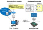
S2C also facilitates the application of large amounts of prototype verification date to the FPGA prototype from a host CPU with its integrated ProtoBridge.  The user developed verification data can take the form of a stream of processor transactions, video data, Wi-Fi/Bluetooth radio data, or directed test patterns.  ProtoBridge interfaces with the FPGA prototype over Ethernet from the host CPU through an AXI-4 master/slave interface embedded in the FPGA, and transfers data to the FPGA prototype at 4GBS using API function calls running on the host CPU.

S2C simplifies quick implementation of the prototyping platform infrastructure with a library of what it refers to as Prototype-Ready IP daughter cards, cables, and connector adapters that support standards-based I/O (PCI, USB, SATA, HDMI, MIPI, GPIO, etc.), adapters for ARM processors (Juno and Zynq), and additional system memory – see the S2C website at http://s2ceda.com/en/product-prototyping-prip.

If you are contemplating an FPGA prototyping project for SoC design development, take a look at S2C’s complete FPGA prototyping solutions – and take the time up-front for some careful thought to a good Plan, choosing a proven platform (like S2C), and experienced prototyping project leadership.

Also Read:

S2C FPGA Prototyping solutions help accelerate 3D visual AI chip

Prototypical II PDF is now available!

StarFive Surpasses Development Goal with the Prodigy Rapid Prototyping System from S2C


Samtec, Otava and Avnet Team Up to Tame 5G Deployment Hurdles

Samtec, Otava and Avnet Team Up to Tame 5G Deployment Hurdles
by Mike Gianfagna on 10-20-2021 at 10:00 am

Samtec Otava and Avnet Team Up to Tame 5G Deployment Hurdles

Everyone is talking about 5G deployment. The promises and the hype are finally turning into reality and products. While excitement is appropriate, victory is not yet in hand. There are still technical hurdles to conquer before the full potential of 5G is realized. In this post, I’ll explore one such challenge – the reliable use of millimeter wave (mmWave) technology for beamforming. You will see how Samtec, Otava and Avnet team up to tame 5G deployment hurdles.

Profile of the Technology

A recent article from Electronic Products does a good job profiling the challenges being addressed by Samtec and Otava. The lead statement in the article summarizes it well:

Unlocking the potential of 5G everywhere with ultra-fast mmWave speeds and low latency requires solving fundamental challenges around range, signal blockers, and proximity to a 5G tower or small cell.

The article goes on to discuss how mmWave frequencies from 24-GHz to 40-GHz hold promise for fast, low latency 5G networks. This technology does present substantial RF propagation challenges.  To realize super-fast 5G network deployment at scale, designers must solve these problems.  The challenges of deployment here can be summarized in one statement, mmWave 5G signals are fragile.

By fragile, I mean they are very short-range. The referenced article explains that, to receive mmWave signals, you need to be within a block or two of a 5G tower with no line-of-sight obstructions. Signals are easily blocked by buildings, walls, windows, and trees. The whole thing can give designers a headache very quickly.  It turns out a promising method to deal with these issues is to use something called beamforming.

If you’re thinking the problem is solved by beamforming, think again. A bit of background is useful for those not following the technology. Beamforming is a technique that focuses a wireless signal at a target as opposed to having the signal radiate in all directions from a broadcast antenna. This results in a more direct connection that is faster and more reliable than it would be without beamforming. The science of beamforming is quite complex. There are many design challenges to be tamed here, and a lot of them are caused by real-world topology. If you want to dig into these challenges, this article from Avnet is a good place to start.

Profile of the Players

With that background out of the way, let’s examine the companies who are collaborating to deliver a solution.

SemiWiki readers should already know about Samtec. They are the company that develops the physical elements of high-performance channels – cables built out of all kinds of materials and connectors with the same broad pedigree. You can catch up on SemiWiki coverage of Samtec here. If you’re trying to build high-performance communication systems (like 5G networks), you will definitely need Samtec’s products, models and technical support.

Otava is a company focused on end-to-end development of technologies used by advanced 5G commercial and DoD applications. The organization’s core competence is phased array system and electronic design. Their portfolio includes transceivers, tunable filters, switches and, you guessed it by now, beamformer technology.

To complete the picture is Avnet, the 900-pound gorilla of distribution and support for a broad range of technology. Both Samtec and Otava are partners of Avent.

Profile of the Solution

By now, you might be thinking that the only way to tame the challenges of 5G transmission is to develop a beamforming approach that is adapted to the conditions being observed. The ability to prototype various approaches to solve the problem would be very useful. The Otava Beamformer IC Evaluation Kit, available from Avnet, is just what you should be looking for. The kit contains everything you need to prototype various beamforming solutions and test them in a real-world setting. Components in the kit include:

  • Otava Beamformer IC Eval Board
  • MicroZed 7010 Xilinx Zynq SOM
  • Modified MicroZed I/O Carrier Card
  • Two custom cable assemblies from Samtec
  • C# GUI

To Learn More

There is a great video on the Avnet solution page where Samtec and Otava explain the capabilities of the kit, with suggested use models.  You can also learn more about Samtec’s precision RF capabilities here. Matt Burns of Samtec recently wrote a great blog that provides another level of detail on the solutions available from Samtec and Otava, complete with photos of the boards. You can check out this informative blog here. Now you know how Samtec, Otava and Avnet team up to tame 5G deployment hurdles.


Its all about the Transistors- 57 Billion reasons why Apple/TSMC are crushing it

Its all about the Transistors- 57 Billion reasons why Apple/TSMC are crushing it
by Robert Maire on 10-20-2021 at 8:00 am

Apple M1

The Apple event today was essentially a reveal of the latest and greatest silicon coming out of the Apple/TSMC partnership and how far ahead of everything else it is. The Mac was simply an aluminum container for the new silicon.

More importantly the event and specs of the TWO new chips, the M1 Pro and the M1 Max demonstrate that the M1 was just the beginning of a large suite of silicon much as we saw in the iPhone lineup. The newly announced silicon is not just a small incremental increase in capability over the original M1 that we have seen out of Intel’s recent product line announcements but a Moore’s Law leap that we are used to from the past generational silicon changes. It harkens back to the type of performance increases we used to see out of Intel before they stumbled.

Catching an accelerating Apple/TSMC just got harder

We have pointed out in prior articles that Intel catching TSMC is going to be tough as TSMC really hasn’t stumbled at all. Given the incremental increase over the Apple M1 announced a year ago, it feels as if the Apple/TSMC partnership may be extending its lead not just keeping pace with innovation.
It may look very ugly if AMD and Intel are fighting over second place with tit for tat incremental changes while Apple accelerates away.

Apple has more than proven its chops in silicon design

Much was said about the legendary “Tick Tock” (no, not the phone app) of Intel’s alternating design and manufacturing enhancement cadence, alternating with the two year lock step of Moore’s Law.

We have also heard more recently about AMD’s design prowess and thinking outside the box.

Jim Keller, the Guru/pied piper genius of CPU design has bounced around the industry from DEC to AMD, Tesla, Intel and Apple sprinkling the fairy dust of magical CPU design wide and far.

Apple has proven that their chip design is not beginners luck nor a one hit wonder but rather a deep bench of capability and expertise and perhaps most importantly the ability to work with a manufacturing partner as if they were a seamless “IDM” .

This also underscores that while design is important its all about manufacturing and Moore’s Law that makes the difference…. but then again we and Intel have known this for a very long time.

Apple Silicon helped it win phone wars… Will it win laptop wars?

The Apple “A” series of processors used in its iPhones are the most advanced in the industry by far. They are perhaps the key factor enabling the leading performance, features and battery life that keep Apple products at a price premium in a leadership, position.

As the “M” series of processors rolls out across the spectrum of Mac computers we will likely see a similar performance advantage that will keep Apple computers in the forefront.

We would also remind everyone that all of Apples products, its watch, earpods, speakers etc; etc; all have smart silicon that differentiates them from otherwise pedestrian versions of similar products.

The Intel doth protest too much….

Intel has been on an anti-Apple PR campaign recently trying unsuccessfully to dull the impact of Apple’s switch away from Intel. There has been significantly blowback and negative reaction from the campaign which was perhaps looking to head off today’s launch of new Macs/Apple silicon. Unfortunately it just underscores the switch and Apple’s success in the silicon business.

Apple Semiconductor

We had suggested a long time ago that perhaps Apple should be considered a semiconductor company or perhaps consider finding a way to monetize that expertise in addition to inside its current product line.

Why wouldn’t it make sense to see Apple chips in servers (running at very low power which is critical in data centers) or selling its chips/expertise to Facebook or “frenemy” google .

Don’t be surprised if we hear about Apple chips going into Apple’s own vast cloud computing complex. it would be a great proving ground.

The Stocks

The event today was a great demonstration of why Apple is where it is and where its going, and why its staying ahead.

They obviously very much understand the importance of silicon, both design and manufacturing and are working hard to use it to their advantage.

Investors need to look beyond this being a Mac roll out and more of a demonstration of their underlying technology advantage and commitment which will keep them ahead.

It should also been seen by Intel that they have their work cut out for them. Apple and TSMC are fast moving targets that have both very deep resources and don’t make a lot of mistakes. They are well managed with the right underlying strategy that understand what makes the markets tick. This is going to be a long hard struggle over many years.

Everyone just has to remember….

“its all about the transistors”

Also Read:

Semiconductors – Limiting Factors; Supply Chain & Talent- Will Limit Stock Upside

ASML is the key to Intel’s Resurrection Just like ASML helped TSMC beat Intel

KLA – Chip process control outgrowing fabrication tools as capacity needs grow


Neural Network Growth Requires Unprecedented Semiconductor Scaling

Neural Network Growth Requires Unprecedented Semiconductor Scaling
by Tom Simon on 10-20-2021 at 6:00 am

Neural Network Growth

The truth is that we are just at the beginning of the Artificial Intelligent (AI) revolution. The capabilities of AI are just now starting to show hints of what the future holds. For instance, cars are using large complex neural network models to not only understand their environment, but to also steer and control themselves. For any application there must be training data to create useful networks. The size of both the training and inference operations are growing rapidly as useful real-world data is incorporated into models. Let’s look at the growth of models over recent years to understand how this drives the needs for processing power for training and inference.

Neural Network Growth

In a presentation at the Ansys 2021 Ideas Digital Forum, the VP of Engineering at Cerebras, Dhiraj Mallik, provided some insight into the growth of neural network models. In the last two years model size has grown 1000X, from BERT Base (110 MB) to GPT-3 (175 GB). And in the offing, there is the MSFT-1T model, with a size of 1 TB. The GPT-3 model – which is an interesting topic of its own – was trained with conventional hardware using 1024 GPUs for 4 months. It’s a natural language processing (NLP) model that uses most of the text data on the internet and other sources. It was developed by Open AI, and is now the basis for the OpenAI Codex, which is an application that can write useful programming code in several languages from plain language instructions from users. GPT-3 can be used to write short articles that a majority of readers cannot tell were written by an AI program.

As you can see above, running 1024 GPUs for 4 months is not feasible. In his talk titled “Delivering Unprecedented AP Acceleration: Beyond Moore’s Law” Dhiraj makes the point that the advances needed to support this level of semiconductor growth go far and away beyond what we have been used to seeing with Moore’s Law. In response to this perceived market need, Cerebras released their WSE-1, wafer scale AI engine in 2019 – 56 times larger than any chip ever produced. A year and half later they announced the WSE-2, again the largest chip every built with:

  • 6 trillion transistors
  • 850,000 optimized AI cores
  • 40 GB RAM
  • 20 petabytes/s memory bandwidth
  • 220 petabytes fabric bandwidth
  • Built with TSMC’s N7 process
  • A wafer contains 84 dies, each 550 mm2.

The CS-2 system that encapsulates the WSE-2 can fit AI models with 120 trillion parameters. What is even more impressive is that CS-2 systems can be built into 192-unit clusters to provide near linear performance gains. Cerebras has developed a memory subsystem that disaggregates memory and computation to provide better scaling and improved throughput for extremely large models. Cerebras has also developed optimizations for sparsity in training sets, which saves time and power.

Dhiraj’s presentation goes into more detail about their capabilities, especially in the area of scaling efficiently with larger models to maintain throughput and capacity. From a semiconductor perspective it is also interesting to see how Cerebras analyzed the IR drop, electromigration, and ESD signoff on a design that is 2 orders of magnitude bigger than anything else ever attempted by the semiconductor industry. Dhiraj talks about how at each level of the design – tile, block, and full wafer – Cerebras used Ansys RedHawk-SC across multiple CPUs for static and dynamic IR drop signoff. RedHawk-SC was also used for power electromigration and signal electromigration checks. Similarly, they used Ansys Pathfinder for ESD resistance and current density checks.

With a piece of silicon this large at 7nm, the tool decisions are literally “make or break”. Building silicon this disruptive requires a lot of very well considered choices in the development process, and unparalleled capacity is of course a primary concern. Yet, as Dhiraj’s presentation clearly shows, CS-2’s level of increased processing power is necessary to manage the rate of growth we are seeing in AI/ML models. Doubtless we will see innovations that are beyond our imagination today in the field of AI. Just as the web and cloud have altered technology and even society, we can expect the development of new AI technology to change our world in dramatic ways. If you are interested in learning more about the Cerebras silicon, take a look at Dhiraj’s presentation on Ansys IDEAS Digital Forum at www.ansys.com/ideas.

Also Read

SeaScape: EDA Platform for a Distributed Future

Ansys Talks About HFSS EM Solver Breakthroughs

Ansys IDEAS Digital Forum 2021 Offers an Expanded Scope on the Future of Electronic Design


Take the Achronix Speedster7t FPGA for a Test Drive in the Lab

Take the Achronix Speedster7t FPGA for a Test Drive in the Lab
by Mike Gianfagna on 10-19-2021 at 10:00 am

Take the Achronix Speedster7t FPGA for a Test Drive in the Lab

Achronix is known for its high-performance FPGA solutions. In this post, I’ll explore the Speedster7T FPGA. This FPGA family is optimized for high-bandwidth workloads and eliminates performance bottlenecks with an innovative architecture. Built on TSMC’s 7nm FinFET process, the family delivers ASIC-level performance while retaining the full programmability of an FPGA. There is a lot to learn about the Speedster7T. Achronix now has a video available that will answer a lot of those questions. There is a link to that video and more coming, but first let’s see what happens when you take the Achronix Speedster7t FPGA for a test drive in the lab.

Steve Mensor

Steve Mensor, VP of sales and marketing at Achronix introduces the video. Steve has been with Achronix for almost ten years and spent 21 years at Altera before that. He certainly knows a lot about FPGAs – design and application. Steve begins by outlining some of the elements of the previously mentioned innovative architecture. There is a lot of dedicated capability on board the Speedster7T. This includes:

  • 112 Gbps SerDes
  • 400G Ethernet
  • PCIe Gen5
  • GDDR6 running at 4 Tbps
  • DDR 4 running at 3,200 Mbps
  • A proprietary machine learning processor
  • 2D network on chip (NoC)

The proprietary machine learning processor delivers a lot of functionality, including floating point, block floating point and integer operations. The 2D NoC is a new-to-the-industry capability for FPGAs from Achronix. The NoC can route data from any of the high-speed interfaces to the core FPGA fabric at 2 GHz without consuming any of the FPGA logic resources.  All of this on-board technology allows you to get to ASIC-level performance in an FPGA.

Katie Purcell

Steve then hands the presentation over to Katie Purcell, application engineering manager at Achronix. Katie has been with Achronix for four years. Prior to that she was an ASIC designer. She also spent time at Xilinx. Katie is the one who takes the Speedster7t FPGA for a test drive in the lab, and she is definitely up to the challenge.

Katie takes the viewer into the Achronix lab where bring-up of the Speedster7T is being performed – validation and characterization. The demo Katie presents shows the device running 400G ethernet traffic on the Achronix VectorPath accelerator card. Katie begins by summarizing the key elements of the demonstration, which include:

  • 8 X 50G external interface
  • Single 400G interface in ethernet subsystem
  • Data divided to four separate streams in the 2D NoC
  • Each stream processed independently

Katie spends some time on the 2D NoC. She points out that this capability makes the design simpler and easier to close timing. This unique 2D NoC came up several times during the demo. It’s worth digging in a bit more to understand it. Achronix previously presented a webinar about this unique capability that was covered on SemiWiki called 5 Reasons Why a High Performance Reconfigurable SmartNIC Demands a 2D NoC. The good news is that a replay of this very informative webinar is now available. You can watch it here.

Katie takes you through a detailed look at what’s going on inside the Speedster7T device as it processes the data packets. Knowing those details helps to understand the ease of setup and delivered accuracy that is shown during the demo. If you think a unique device like this could help your design project, I highly recommend you watch the demo. It’s short, but very useful. You can access the demo video here.

Now you know how to take the Achronix Speedster7t FPGA for a test drive in the lab. You can find out more details about this unique FPGA family here.


Using PUFs for Random Number Generation

Using PUFs for Random Number Generation
by Kalar Rajendiran on 10-19-2021 at 6:00 am

3 API Functions

In our daily lives, few of us if any, would want randomness to play any role. We look for predictability in order to plan our lives. But reality is that random numbers have been playing a role in our lives for a long time. The more conspicuous use cases of random numbers are with key fobs, and nowadays mobile phones. And then there are a whole lot of behind the scene use cases that leverage random numbers for security purposes. As such, generating true random numbers is a topic of ongoing interest within the field of math and computer science.

There have been instances where faulty random number generators caused security and authentication issues. Nonces are random numbers used in authentication protocols. The term nonce as used here carries the meaning “number only used once.” Not to be mixed up with the slang meaning of this word as used in some parts of the world. There have been incidents in the past where a nonce was generated more than once due to weak random number generators. Lot of progress has been made since then and such lapses don’t happen as much. Nonetheless, due to the explosive growth in internet linked devices, we face increasing levels of threats to device and information security.

It is in this context that the recent announcement by Intrinsic ID of a NIST-Certified  Software Random Number Generator (RNG) is of interest. You can read the press release “Intrinsic ID Announces NIST-Certified Software Random Number Generator (Zign RNG) for IoT Devices” here. It points to a report that has identified critical vulnerabilities in billions of IoT devices due to poor random number generation mechanisms. The announcement states that their Zign RNG ensures a source of true randomness addressing the critical security flaw in IoT devices. And that the Zign RNG is the industry’s first and only embedded RNG software solution.

One of the coveted features of any solution is its ability to be a drop-in replacement without requiring any hardware change to already designed and manufactured devices. Particularly those that are already deployed in the field. Zign RNG claims to be such a solution, a cryptographically secure NIST-certified RNG that can even be retrofitted on already-deployed devices.

The curiosity in all of us would want to know how is Intrinsic ID able to achieve the above claimed solution. The answer can be found in the webinar that Intrinsic ID recently hosted on PUF Café. The webinar was titled “Using PUFs for Random Number Generation” and was delivered by Dr. Nicolas Moro. He is an embedded security systems engineer at Intrinsic ID. This blog is a synthesis of the salient points from watching that webinar.


Attractiveness of SRAM PUF for RNG

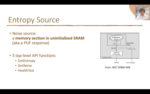
PUFs can be seen as the fingerprint of a device. In the case of SRAM PUFs – like most PUFs – this fingerprint comes with noise. In the normal use case of a PUF, algorithms are used to remove this noise. On the other hand, random number generators need a non-deterministic source of entropy. And the noise from an SRAM PUF fingerprint can be used for that purpose. Given that we know that every IoT device already contains SRAM, it makes sense to use the noise from the SRAM PUF as a source of entropy to extract a true random seed. Not only that, SRAM has additional benefits as seen in the Figure below.


Harvesting the Entropy for RNG

The non-deterministic part of the start-up values of the SRAM is used as a source of entropy. This entropy is used as a seed for a Deterministic Random Bit Generator (DRBG).

The output of an SRAM PUF is slightly different each time. Random and repeatable but not 100% repeatable. For PUF purposes, this noise is eliminated through error correction techniques. But for random number generation, the data derived from the noise needs to pass some statistical tests. Thus, some processing is needed to create the seed for the DRBG.

The SRAM PUF source has enough noise in it to be able to generate the right number of bits of entropy for desired levels of security. For example, Intrinsic ID has established through its experiments that only 2 kilobytes of uninitialized SRAM are required to get 192 bits of entropy.


PUF-based RNG

The National Institute of Standards and Technology (NIST) has established clear set of specifications for secure random number generators. Refer to Figure below for the specification for each topic relating to this subject matter.


The entropy derived from the PUF is fed as the seed to a DRBG to yield random data. A maximum of 2^19 bits can be received per call to the DRBG. The maximum number of calls that can be made before the reseed counter runs out is 2^48. That is more than 281 trillion calls. Everyone would agree that is large number. In the event the counter does run out, a power reboot of the device would start it off with new entropy to reseed the DRBG.

For implementing a 128-bit security level, a total of 192 bits of entropy is needed from the SRAM PUF. As noted earlier, this is achievable with just 2kilobytes of uninitialized SRAM. Once the seeding is one, this 2kilobytes of memory is available for other uses and purposes within the application.


NIST Certification

NIST has qualified third party certification labs to conduct validation programs. The Cryptographic Algorithm Validation Program (CAVP) is for certifying the RNG algorithm. The Cryptographic Module Validation Program (CMVP) is for certifying the system/module that implements and uses the algorithm. In addition to a GetEntropy function, a RNG solution must include a GetNoise and a HealthTest function. These are requirements by NIST and must be made available through an API at the top level. Refer to Figure below.


The GetEntropy function is of course the one that returns the seed for the DRBG.

The GetNoise function is for use by a third-party certification lab during their evaluation to check the entropy source behavior against the specification.

The HealthTest function is used during run time to protect against any catastrophic failures. For example, if during run time, all zeroes are received as input for seeding DRBG, it will abort and raise a flag.


Summary

Zign RNG software can be implemented at any stage of a device’s lifecycle, even after a device is already deployed in the field. It has passed all standard NIST randomness tests and is a NIST/FIPS-compliant software solution. It addresses the issue of hardware RNG peripherals used in IoT devices running out of entropy and leaving the devices vulnerable.

Intrinsic ID’s Zign RNG is available now and is applicable to anyone making IoT devices or chips for IoT. More details about the product can be accessed here and a product brief can be downloaded from here.

You can access the full press release of the Zign RNG product announcement here.

And you can watch and listen to the webinar by registering here at PUF Café.

Also Read:

Quantum Computing and Threats to Secure Communication

Webinar: How to Protect Sensitive Data with Silicon Fingerprints

CEO Interview: Pim Tuyls of Intrinsic ID


APR Tool Gets a Speed Boost and Uses Less RAM

APR Tool Gets a Speed Boost and Uses Less RAM
by Daniel Payne on 10-18-2021 at 10:00 am

Aprisa

Automatic Place and Route (APR) tools have been around since the 1980s for IC design teams to use, and before that routing was done manually by very patient layout designers. Initially the big IDMs had their own internal CAD groups coding APR tools in house, but eventually the commercial EDA market picked up this automation area, and it’s been a highly competitive segment ever since then. Users of APR tools have a few metrics that they follow closely:

  • Capacity, # of cells in a block
  • Runtime
  • Quality of Results, did I meet area, timing and power goals?
  • Memory usage
  • Number of DRC violations to fix after APR

I just had a video call with Henry Chang at Siemens EDA about their latest APR tool release of Aprisa 21.R1, and it was an eye opener.  On capacity, he mentioned that many users run blocks in Aprisa that are 3-4 million instances, although some teams prefer to run larger blocks with 8-9 million instances. The tool can be run in either flat or hierarchical mode, and the big news is that on the largest designs the run times are up to 2X faster than the previous release. So, how did they do that?

Aprisa

You may recall that Siemens EDA acquired Avatar last year, July 2020. The engineers working on the previous routing tool Nitro combined to work on Aprisa, and then management hired even more developers to get the runtime improvements, so developer headcount increased by more than 2X. Not only did the runtime improve by an average of 30% for all designs, but the RAM usage decreased by up to 60% as well. Most APR jobs are run locally on a big server, so being more efficient is attractive to engineering departments., especially when their biggest jobs can run for a few days.

Aprisa developers improved pretty much all parts of the tool:

  • Placement optimization
  • Clock Tree Synthesis (CTS) optimization
  • Route optimization
  • Timing analysis

APR, like most critical EDA tools goes through a qualification process at the foundries, and Aprisa is fully certified for the TSMC 6nm process, while the 5nm and 4nm nodes have implemented all of the required design rules and features, so stay tuned for the official announcement of qualifications for these nodes.

Modern SoCs often use multi-power domains (MPD), and Aprisa handles that too.  It sounds like the QoR with Aprisa come about in part by their approach to detailed routing, and there’s a previous blog on that topic.

Henry Chang

I first met Henry at Mentor Graphics, back in 2000, when we worked on a Fast-SPICE circuit simulator called Mach TA. He started his EDA career in 1993 as a co-founder and architect at Anagram, and had stints at Avant! and Atoptech, so he really understands the IC design process from SPICE to AMS and APR.

Summary

APR tool users have choices when it comes to finding and using a leading-edge tool for design implementation, and having a multi-vendor tool flow is a solid choice. Siemens EDA has bulked up their Aprisa team, and the improvements that are now revealed  in faster run times, with a smaller memory footprint look impressive, with foundry support qualified at 6nm, and a pipeline to include 5nm and 4nm nodes well underway. Read the press release online.

Related Blogs


IEDM 2021 – Back to in Person

IEDM 2021 – Back to in Person
by Scotten Jones on 10-18-2021 at 6:00 am

IEDM 2021 SemiWIki

Anyone who has read my previous articles about IEDM knows I consider it the premier conference on process technology.

Last year due to COVID IEDM was virtual and although virtual offers some advantages the hallway conversations that can be such an important part of the conference are lost. This year IEDM is returning as a live event in San Francisco from Dec. 11-15, 2020, with on-demand access to materials starting Dec. 17.

Saturday, December 11 will be the tutorials:

90-Minute Tutorials – Saturday, Dec. 11

The 90-minute Saturday tutorial sessions on emerging technologies have become a popular and growing part of the IEEE IEDM. They are presented by experts in the field to bridge the gap between textbook-level knowledge and leading-edge current research, and to introduce attendees to new fields of interest:

2:45 p.m. – 4:15 p.m.

4:30 p.m. – 6:00 p.m.

Sunday, December will be the short courses:

IEDM Short Courses – Sunday, Dec. 12

In contrast to the Tutorials, the full-day Short Courses are focused on a single technical topic. Early registration is recommended, as they are often sold out. They offer the opportunity to learn about important areas and developments, and to network with global experts.

  • Future Scaling and Integration Technology, organized by Dechao Guo, IBM Research


Practical Implementation of Wireless Power Transfer, Hubregt Visser, IMEC

Monday will begin the conference with the plenary talks:

Plenary Presentations – Monday, Dec. 13

  • The Smallest Engine Transforming Our Future: Our Journey Into Eternity Has Only Begun, Kinam Kim, Vice Chairman & CEO, Samsung Electronics Device Solutions Division
  • Creating the Future: Augmented Reality, the Next Human-Machine Interface, Michael Abrash, Chief Scientist, Facebook Reality Labs
  • Quantum Computing Technology, Heike Riel, Head of Science & Technology, IBM Research and IBM Fellow

Followed by the full conference Monday through Thursday.

As every year, IEEE IEDM 2021 will offer Special Focus Sessions on emerging topics with invited talks from world experts to highlight the latest developments.

Monday, December 13, 1:35 PM

Session 3 – Advanced Logic Technology – Focus Session – Stacking of devices, circuits, chips: design, fabrication, metrology – challenges and opportunities

Tuesday, December 14, 9:05 AM

Session 14 – Emerging Device and Compute Technology – Focus Session – Device Technology for Quantum Computing

Wednesday, December 15, 9:05 AM

Session 25 – Memory Technology/Advanced Logic Technology – Focus Session – STCO for memory-centric computing and 3D integration

Wednesday, December 15, 1:35 PM

Session 35 – Sensors, MEMS, and Bioelectronics/Optoelectronics, Displays, and Imaging Systems – Focus Session – Technologies for VR and Intelligence Sensors

Session 38 – Emerging Device and Compute Technology/Optoelectronics, Displays, and Imaging Systems – Focus Session – Topological Materials, Devices, and Systems

For more information and to access the full program as it becomes available, please go to: https://www.ieee-iedm.org/

IEEE International Electron Devices Meeting (IEDM) is the world’s preeminent forum for reporting technological breakthroughs in the areas of semiconductor and electronic device technology, design, manufacturing, physics, and modeling. IEDM is the flagship conference for nanometer-scale CMOS transistor technology, advanced memory, displays, sensors, MEMS devices, novel quantum and nano-scale devices and phenomenology, optoelectronics, devices for power and energy harvesting, high-speed devices, as well as process technology and device modeling and simulation.


Silicon Startups, Arm Yourself and Catalyze Your Success…. Spotlight: Semiconductor Conferences

Silicon Startups, Arm Yourself and Catalyze Your Success…. Spotlight: Semiconductor Conferences
by Kalar Rajendiran on 10-17-2021 at 10:00 am

Live Panel

The arrival of fall seems to typically raise the number of conferences hosted by semiconductor ecosystem companies. The conferences may go by different names. But whether called a forum, summit, conference, or by some other creative name, the purpose is the same. It is to bring together technologists and business people together to share ideas. More specifically, to discuss industry opportunities and challenges and of course to tout the respective ecosystem partners’ accomplishments. Samsung Foundry Forum and Global Foundries Technology Summit were held in September. October has some interesting ones too.

As important as it is for everyone within the industry to participate in these conferences, the value for smaller companies is potentially much higher. Why? Because, where else and how else would a smaller company with smaller financial resources be able to get this, compressed into a few days, all happening in one location? Of course, nowadays, that one location happens to be a virtual one, in many cases. That is even better.

Just because something is free and you can attend it without even leaving your home or office does not mean you should or could attend all these conferences. So, how do you go about choosing? Well, to some extent it depends on who you are, where you are in terms of your product idea and what kind of assistance and insights you would need for that stage.

Leveraging Conference Opportunities

Arm Dev Summit

One that is in the immediate offing is the Arm Dev Summit, scheduled as a virtual event for Oct 19-Oct 21, 2021. There, you will get a chance to network with Arm’s global community of hardware designers and software developers. And an opportunity to hone your ideas, whether it is in AI, IoT, 5G, wired communications or super-computing. It’s a 3-day virtual event and the agenda is extensive. Whether you are just starting up, simply crazy about autonomous vehicles, a myth buster type or for that matter a 5G Campfire kind of person, there is something of value for everyone. Arm’s entire ethos is about creating diverse, multi-participant ecosystem to unlock new possibilities.

Register and attend all sessions that are relevant to your areas of interest. If you are a startup, you would certainly want to check out the following back-to-back sessions. Attend a live panel session that will focus on helping startups succeed, followed by a networking session with the same theme.

Of course, navigating a startup to market success demands lot more than just attending developer conferences. Building investor confidence for securing early rounds of funding is key. Innovating while keeping costs down is essential. Flexibility to test and iterate without overrunning the budget would be a big advantage. Reducing the risk in the project and product schedules cannot be understated. Getting a product to market faster than the competition is crucial. A series of future blogs will tackle these topics and how Arm and Silicon Catalyst could be of help.

TSMC OIP Forum

If you’re looking at the siliconization aspects of your products, you would want to register for the TSMC Open Innovation Platform (OIP) Forum. This one is scheduled for Oct 26, 2021 for the Americas Time Zone and for Oct 27, 2021 for Europe and Asia Time Zones. You can register for TSMC OIP Forum using this link.

Snapshot of some Sessions: TSMC OIP Forum, Oct 26, 2021

Catalyzing Your Business

Attending the right conferences certainly is helpful. But if you’re an emerging startup, you could benefit from more help on an ongoing basis, at least until you gain escape velocity.

Silicon Valley is known all over the world and semiconductors are the life force behind all electronics. All the modern conveniences we take for granted are powered by advanced and complex chips. And designing, manufacturing and producing these chips in high volumes are challenging tasks. Yet, there are no incubators focused on semiconductors. Although hard to believe, it is true.

Silicon Catalyst is the world’s only incubator focused on semiconductor solutions, including MEMS, sensors and intellectual property. Silicon Catalyst’s mission is to help semiconductor startups succeed. Through a coalition of in-kind and strategic partners, investors and advisors, Silicon Catalyst helps startups accelerate their ideas through prototypes, and onto a path to volume production.

As a strategic and in-kind partner, Arm participates in the incubation selection process and actively looks for opportunities to partner with these startups. As an in-kind partner, TSMC provides MPW shuttles for companies in the incubator. The Silicon Catalyst coalition provides everything startups need to design, fabricate, and market semiconductor solutions. The startups gain millions of dollars’ worth of EDA tools, IP, PDKs, prototypes, design and test services, packaging and business solutions and expert guidance from accomplished advisors. For more details, check out the full list of Silicon Catalyst partners.

Upcoming Blog Series

This blog is the first piece in a series of blogs to follow. The future blogs will cover challenges and opportunities that silicon startups commonly face and how the Silicon Catalyst ecosystem can be of significant help in accelerating their growth. The primary goal of the blog series is to identify tried-and-true solutions to the many problems to be faced, ultimately helping accelerate a silicon startup’s transformation from the initial conceptual stage to business success in the market.

Also Read:

WEBINAR: Maximizing Exit Valuations for Technology Companies

Silicon Catalyst and Cornell University Are Expanding Opportunities for Startups Like Geegah

Silicon Catalyst is Bringing Its Unique Startup Platform to the UK