
Each year, TSMC conducts two events – the Technology symposium in the Spring and the Open Innovation Platform (OIP) ® Ecosystem Forum in the Fall. Yet, what is the OIP ecosystem? What does it encompass? And, how does the program differentiate TSMC from other foundries? At the recent OIP Forum in Santa Clara, Suk Lee, Senior Director, TSMC Design Infrastructure Management Division, presented a review of OIP, highlighting the breadth of technology and support available for TSMC process nodes. Additionally, and very significantly, he described the extensive engineering investment made to develop and qualify new process design kit materials (PDK) and IP offerings. Here are some of the highlights of Suk’s presentation.
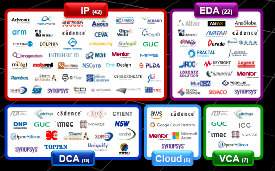
Figure 1. OIP partner overview (Source: TSMC)
OIP entails the collaboration between TSMC and numerous partners, spanning a range of technical facets of silicon foundry support:
- EDA tool providers
- IP developers
- Design Center Alliance (DCA) providers, offering services ranging from system-level front-end design to back-end physical/test implementation
- Value Chain Aggregators (VCA), additional service providers commonly offering a different set of capabilities, including assembly/test and supply chain management support
and, the newest aspect of OIP partnership, which was announced last year with the introduction of its OIP Virtual Design Environment (OIP VDE), lowering entry barriers of Cloud adoption for the customers of all sizes
- Cloud service providers
To perhaps better distinguish between the DCA and VCA partners, Suk overlaid the previous chart on top of the Design Enablement and Process Development groups at TSMC – see the figure below.
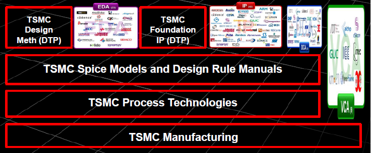
Figure 2. OIP partner interactions with TSMC R&D (Source: TSMC)
Yet, these OIP designations are much more than companies enrolling with TSMC. Suk emphasized the qualification requirements and ongoing monitoring to which each OIP partner is subjected, as illustrated below.
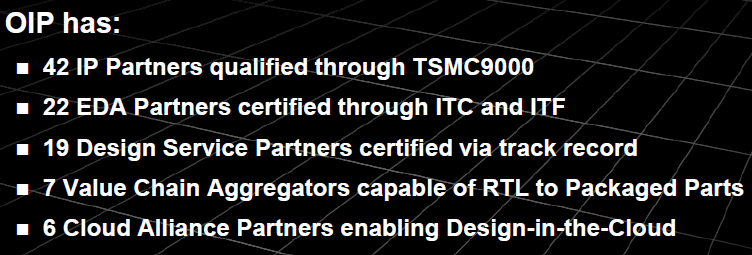
Figure 3. Examples of OIP partner qualification requirements (Source: TSMC)
From TSMC’s own derivative of ISO9000 qualify management and assurance (aka, TSMC9000) to qualification of process interconnect technology definitions to ongoing certification of OIP service providers, there is a major emphasis on ensuring foundry customer success.
Perhaps the best illustration of OIP collaboration is the activity pursued with EDA partners during new process development. This activity ensures new tool features and full methodology reference flow capabilities are qualified concurrently with initial process availability for IP developers and early end customer adopters. Suk provided examples where new EDA tool attributes were defined, developed, and integrated into reference flows, driven by both process innovations (e.g., EUV lithography) and design reliability and manufacturability (e.g., via pillars, statistical analysis). The figures below illustrate how the digital and custom design flows from EDA OIP partners were enhanced in support of these advanced process requirements.
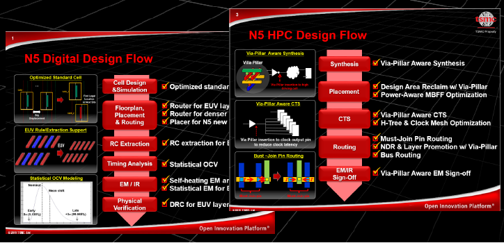
Figure 4. New EDA tool features addressing process requirements – digital flows (Source: TSMC)
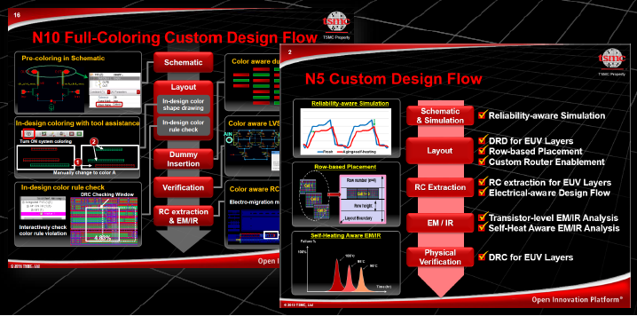
Figure 5. New EDA tool features addressing process requirements – custom implementation flows (Source: TSMC)
Engineers are skeptical by nature, seeking a silicon-proven demonstration of models, EDA tool features, and reference flows. Suk highlighted the specific collaboration with ARM – for nearly a decade, TSMC and ARM have used leading ARM core IP as a testchip vehicle. Full EDA (and IP) qualification reports are available at TSMC’s customer portal. On the day of OIP Forum, the two companies also announced the latest result of their collaboration, an industry-first 7nm silicon-proven chiplet system based on multiple Arm® cores and leveraging TSMC’s Chip-on-Wafer-on-Substrate (CoWoS®) advanced packaging solution.
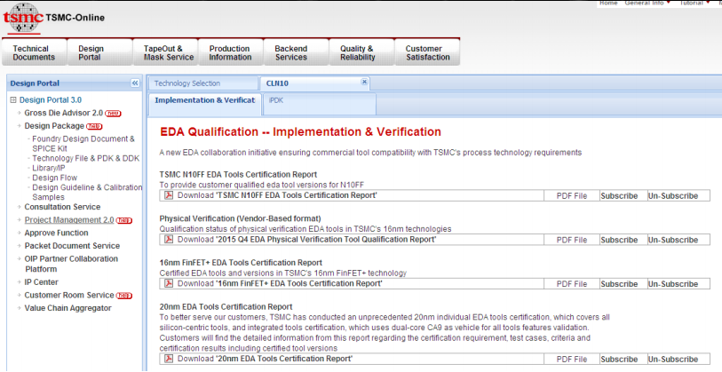
Figure 6. Screenshot of example EDA qualification reports on the TSMC portal (Source: TSMC)
With all the news relative to new process node announcements, it is easy to overlook the underlying activities and resources required to synchronize process availability with the companies supporting the related EDA, IP, and service provider ecosystem. Suk’s presentation reminded the OIP Ecosystem Forum audience of the tremendous investment made as part of the effort to sustain Moore’s Law (for at least another node or two). The focus that TSMC has applied to design enablement has truly been a differentiating characteristic of their corporate philosophy.
Share this post via:


Comments
One Reply to “A Review of TSMC’s OIP Ecosystem”
You must register or log in to view/post comments.