
At the recent Open Innovation Platform® Ecosystem Forum in Santa Clara, TSMC provided an enlightening look into the future of heterogeneous packaging technology. Although the term chiplet packaging is often used to describe the integration of multiple silicon die of potentially widely-varying functionality, this article will use the term heterogeneous packaging. The examples below illustrate integration of both large and small die, DRAM die, and a full high-bandwidth memory die stacks (HBM2), much richer in scope than would commonly be designated as a chiplet. Dr. Douglas Yu, Vice President of Integrated Interconnect and Packaging at TSMC, provided a review of current TSMC heterogeneous packaging offerings, and a 3D package vision that could be best described as “More-than-More-than-Moore”.
Doug began with the well-understood realization that the pace at which the cost-per-transistor has improved with IC process technology scaling has slowed.
![]()
Figure 1. The rate of cost-per-transistor improvements with process technology scaling has slowed. (Source: TSMC)
There are certainly ongoing product PPA benefits to scaling, but the ultimate cost for the total system functionality may drive system designers to pursue heterogeneous packaging alternatives.
CoWoS
The first heterogeneous packaging offering from TSMC was Chip-on-Wafer-on-Substrate ( CoWoS® ). A cross-section of a CoWoS® package is illustrated below.
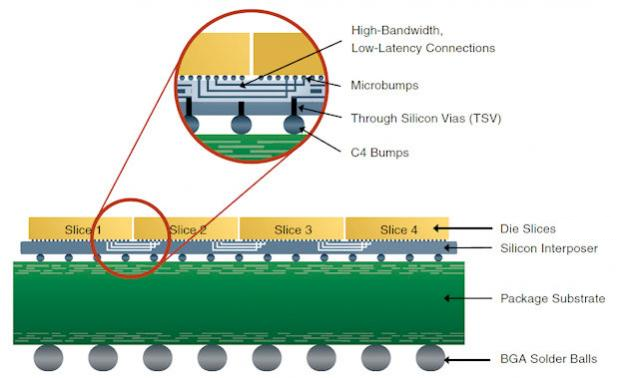
Figure 2. CoWoS® package integration (Source: TSMC)
A silicon interposer provides the interconnects between the die, with through-silicon vias (TSV) to the substrate below. Doug highlighted the recent advances in CoWoS® technology in production, specifically the ability to fabricate the interposer at 2X the max reticle size for wafer lithography.
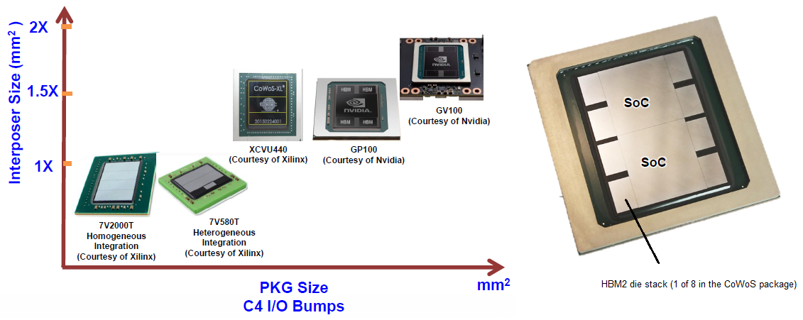
Figure 3. CoWo®S support for a silicon interposer greater than the single max-reticle size (Source: TSMC)
InFO-PoP
Doug reviewed TSMC’s cost effective heterogeneous integration package, based on the Integrated FanOut (InFO) technology. The original InFO offering provided (reconstituted) wafer-level redistribution layer connectivity to extended bump locations outside the die perimeter. The newer InFO-PoP package cross section is illustrated below.
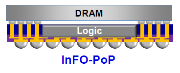
Figure 4. InFO-PoP cross section (Source: TSMC)
The extension of the InFO molded package beyond the embedded die is used for Through-InFO vias (TIV) between the top die and the redistribution layer connections.
SoIC®
A more recent TSMC heterogeneous package innovation involves the transition from microbump connections between die and substrate to a bumpless (thermo-compression) bond between direct die connections – see the figure below for a comparison between microbump and bumpless attach. TSMC-SoIC® is an innovative frontend wafer-process-based platform that integrates multi-chip, multi-tier, multi-function and mix-and-match technologies to enable high speed, high bandwidth, low power, high pitch density, and minimal footprint and stack-height heterogeneous 3D IC integration.
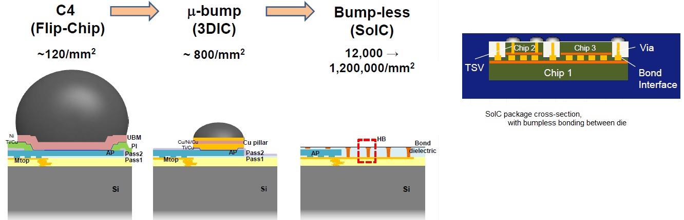
Figure 5. Comparison of bump and bumpless technology characteristics, and SoIC® package cross-section (Source: TSMC)
Through silicon vias provide connection to bumps, part of the final back-end package assembly flow. The density and electrical characteristics of the bumpless attach technology are far superior. (Here’s a previous semiwiki article that describes the TSMC SoIC® package technology – link.)
https://semiwiki.com/semiconductor-manufacturers/tsmc/8150-tsmc-technology-symposium-review-part-ii/
Future Vision
Doug provided a vision for heterogeneous packaging, which combines the unique advantages of the technologies described above. The figure directly below depicts a bumpless SoIC® composite as part of a larger InFO or CoWoS® package, integrating additional die and/or HBM memory stacks.
The second figure below illustrates multiple levels of (thinned) die using bumpless attach for subsequent back-end package assembly. Doug referred to this multi-level SoIC® solution as part of the transition from 3D system integration to full 3D system scaling.
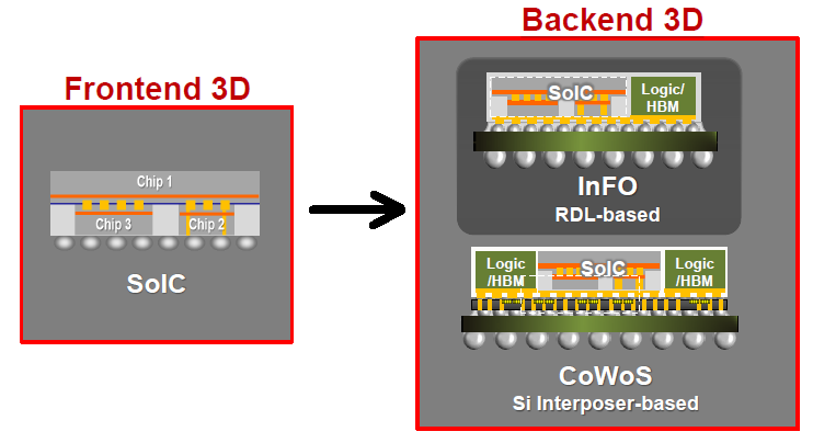
Figure 6. SoIC® integration in a subsequent InFO or CoWoS® package (Source: TSMC)

Figure 7. Multi-level bumpless die integration à 3D system scaling (Source: TSMC)
The heterogeneous packaging technology vision presented by TSMC will truly provide system architects with great opportunities for continued scaling. In addition to traditional monolithic die PPA considerations for technology selection, this vision offers additional opportunities for system-level functional integration and packaging cost optimizations. It will be fascinating to see how these heterogeneous packaging offerings impact future system designs.
Share this post via:


Comments
3 Replies to “A Future Vision for 3D Heterogeneous Packaging”
You must register or log in to view/post comments.