Synopsys 800x100 px High Quality

CDC for MBIST: Who Knew?

CDC for MBIST: Who Knew?
by Bernard Murphy on 11-09-2021 at 6:00 am

CDC for MBIST

Now and again, I enjoy circling back to a topic on which I spent a good deal of time back in my Atrenta days – clock domain crossing analysis (CDC). This is an area that still has opportunity to surprise me at least, in this case looking at CDC analysis around MBIST logic. CDC for MBIST might seem strange. Isn’t everything in test mode synchronous with a single clock? Not quite. JTAG runs on an independent and relatively slow clock whereas MBIST runs on a system speed clock. On the first day of Synopsys Verification Day 2021, Wesley Lee of Samsung gave a nice overview on the details of this unique application of CDC analysis.

Who cares?

CDC is for functional mode problems surely. Who cares if a synchronization error occurs in MBIST testing? Samsung does and good for them. MBIST isn’t just for bring-up testing. High safety level auto electronics now launch periodic inflight testing to check all critical blocks are functioning correctly. MBIST testing would be included in that checklist, but it wouldn’t be very useful if it might be susceptible to synchronization errors. Best case it reports an error on a good memory and your car keeps demanding it be taken in for service. Worst case it fails to report an error on a bad memory…

What’s special about MBIST CDC?

First, Samsung do before and after CDC analyses. “Before” is with master and slave TAP controllers and connections inserted, though with JTAG disabled and without MBIST controllers. “After” is with JTAG enabled and MBIST controllers inserted. Wesley’s rationale for this is that the MBIST logic alone represents a significant addition to the rest of the design. He wants first to flush out problems without MBIST to simplify analysis when MBIST is added.

He mentioned finding value particularly in Machine Learning-based analysis for clustering violations around common root-causes. I remember the early days of combing through thousands of violations, trying to figure out where they all came from. The ML extensions represent a **huge** advance.

Exception analysis

The thing that really stood out for me in Wesley’s talk was optimization of the analysis through quasi static assignments and other constraints. You can be slapdash with these assignments in CDC, but Wesley’s approach is very surgical.

In functional mode, the JTAG interface is obviously static, whereas in MBIST mode, some interface signals can be case analyzed (set to a fixed value). Some signals from slave TAPs to the corresponding MBIST controllers counts as effectively synchronized because they are qualified by an enable signal which is synchronized.

More interesting still, some MBIST signals interface with the slave TAP controller without synchronization or qualification of any kind. You should understand that this design uses a 3rd-party MBIST controller, so Wesley can’t just walk down the hall to ask why. They needed a meeting or two with the supplier to figure out why they considered this approach OK. The supplier explained that the controller knows how long its analysis will take. It counts for that number of clocks, plus a margin and then transmits these signals. In effect the signals are quasi-static until the slave TAP reads these values and again quasi static beyond that point.

Wesley’s summed up by saying that sometimes you must understand programming sequences. Not all quasi-static assignments have no-brainer rationales. Sometimes you really need to dig into the functionality.

A very interesting review of CDC analysis around MBIST. You can learn more from the recorded session. Wesley’s gave his talk on Day 1.

Also Read:

AI and ML for Sanity Regressions

IBM and HPE Keynotes at Synopsys Verification Day

Reliability Analysis for Mission-Critical IC design


A Packet-Based Approach for Optimal Neural Network Acceleration

A Packet-Based Approach for Optimal Neural Network Acceleration
by Kalar Rajendiran on 11-08-2021 at 10:00 am

6 Optimal Work Unit Designed for DLA

The Linley Group held its Fall Processor Conference 2021 last week. There were a number of very informative talks from various companies updating the audience on the latest research and development work happening in the industry. The presentations were categorized as per their focus, under eight different sessions. The sessions topics were, Applying Programmable Logic to AI Inference, SoC Design, Edge-AI Software, High-Performance Processors, Low-Power Sensing & AI, Server Acceleration, Edge-AI Processing, High-Performance Processor Design.

Edge-AI processing has been garnering a lot of attention over the recent years and hardware accelerators are being designed-in for this important function. One of the presentations within the Edge-AI Processing session was titled “A Packet-based Approach for Optimal Neural Network Acceleration.” The talk was given by Sharad Chole, Co-Founder and Chief Scientist at Expedera, Inc. Sharad makes a strong case for rethinking implementation of Deep Learning Acceleration (DLA). He presents details of Expedera’s DLA platform and how their packet-based accelerator solution enables optimal results. The following is what I gathered from Expedera’s presentation at the conference.

Market Needs

As fast as the market for edge processing is growing, the performance, power and cost requirements of these applications are also getting increasingly demanding. And AI adoption is pushing processing requirement more toward data manipulation rather than general purpose computing. Deep learning models are fast evolving and an ideal accelerator solution optimizes for many different metrics. Hardware accelerator solutions are being sought after to meet the needs of a growing number of consumer and commercial applications.

Inefficiencies in Neural Network Acceleration

Traditional DLA architectures breakdown neural networks (NN) into granular work units for execution. This approach directly limits performance as existing hardware cannot directly execute higher level functions. While CPU-centric solutions may offer flexibility and potential for optimization, they are non-deterministic and fall short on power efficiency. Interpreter-centric solutions offer layer-level reordering optimization but they require large amounts of on-chip memory, a resource that is precious, particularly in edge devices. Benchmark studies indicate that current AI inference SoCs are performing at 20-40% utilization levels. Efforts to improve performance efficiency often prove counterproductive. For example, increasing throughput with larger batch sizes adversely impacts latency. Improving accuracy with compute precision consumes additional bandwidth and power. Targeting higher system utilization increases software complexity. Deploying trained models using these solutions is cumbersome and time-consuming.

Packet-based Approach for NN Acceleration

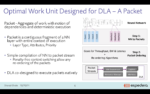
To overcome the above inefficiencies, Expedera breaks down NN into optimal work units designed for its DLA, calling them packets. Packets in this context are defined as contiguous fragments of NN layers, along with the respective contexts and dependencies. Packets allow for simple compilation of the neural network into packet streams. The packet streams are executed natively on the Expedera DLA platform.

This packet-based approach renders lots of benefits. The design is simplified and performance is improved. The amount of memory and bandwidth requirements are drastically reduced, allowing DLA hardware to be better right-sized. For example, using a popular benchmark the packet-based approach was shown to reduce DDR transfers by more than 5x compared to layer-based processing. The packet-based approach provided cascading benefits including fewer intermediate data movement, higher throughput, lower system power requirement, and reduced BOM cost.

Expedera’s Solutions

As edge processing workloads evolve, applications need to support multiple models and increasing data rates. And SoCs need to support a mix of applications. The packet-based DLA codesign approach delivers a high-performance solution that is scalable and power efficient. It allows for parallel use of independent resources. Expedera DLA enables zero-cost context switching and provides for multi-tenant application support.

Expedera’s Compiler achieves out-of-the-box high performance. Its Estimator allows for right-sizing the DLA hardware. The Runtime scheduler orchestrates the best sequence of NN segments based on application requirements, enabling seamless deployments.

Benefits of Expedera’s DLA Platform

  • Best performance per Watt
  • Smaller designs
  • Lower power
  • Determinism

A Deterministic Advantage

As the packets are complete with context and dependencies, the packet-stream approach guarantees cycle-accurate DLA performance. Packet-DLA codesign enables deterministic and high performant compilation. Exact execution cycles as well as memory and bandwidth needs are known ahead of time, leading to a deterministic execution. This is a prized advantage with edge applications where low and consistent latency is important.

Summary

In a nutshell, Expedera’s customers can easily and rapidly implement their AI SoC designs for edge processing to deliver optimal deep learning acceleration for their applications. Achieving optimal AI performance calls for solving a multi-dimensional problem. With a comprehensive SDK built on Apache TVM, Expedera accelerator IP platform enables ideal accelerator configuration selection, accurate NN quantization and seamless deployment.

To learn about how Expedera’s DLA IP performance compares against other DLA IP solutions, refer to a whitepaper published by the Linley Group. The whitepaper titled “Expedera Redefines AI Acceleration for the Edge” can be downloaded from here.

** Apache TVM is an open-source machine learning compiler framework for CPUs, GPUs, and machine learning accelerators.

Also read:

CEO Interview: Da Chaung of Expedera

Expedera Wiki


S2C EDA Delivers on Plan to Scale-Up FPGA Prototyping Platforms to Billions of Gates

S2C EDA Delivers on Plan to Scale-Up FPGA Prototyping Platforms to Billions of Gates
by Daniel Nenni on 11-08-2021 at 6:00 am

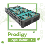
S2C EDA Prodigy Logix Matrix LX2

S2C has been a global leader in FPGA prototyping for nearly two decades now, and its FPGA prototyping platforms have closely tracked the availability of the latest FPGAs – including the latest FPGAs from both Xilinx and Intel.  And they are definitely delivering on the promise to advance their prototyping solutions for hyperscale design prototyping – scaling-up prototyping platform capacities and capabilities to support multi-billion gate designs.

Looking back to early 4Q 2020, S2C announced support for the then-new Xilinx VU19P UltraScale+ FPGAs, offering single, dual, and quad FPGA prototyping platforms.  Then, in December of 2020, S2C followed-up with an announcement of its high-density Prodigy Logic Matrix family of prototyping platforms with 8 FPGAs per Logic Matrix, 8 Logic Matrix per single server rack (64 FPGAs), and the connection of multiple server racks together.  The first iterations of Logic Matrix were delivered with Xilinx VU440 FPGAs (dubbed the LX1) to early customers who couldn’t wait for the VU19P version (dubbed the LX2).

Now, S2C is stepping up its Logic Matrix game with the LX2, which jumps prototyping usable gate capacity by 60% over than the VU440 version!  More usable gates per FPGA means fewer FPGAs, fewer FPGA interconnects, and higher performance for the same prototyped design.  With an estimated gate capacity of 392 million gates per LX2, a fully populated standard server rack with 8 LX2’s enables an estimated prototyping capacity of over 3 billion ASIC gates!

Figure 1: Prodigy Logic Matrix LX2

Prodigy Logic Matrix Family
LX1 LX2
FPGA XCVU440 XCVU19P
Estimated ASIC Gates (M) 240 392
Number of FPGAs 8 8
System Logic Cells (K) 44,328 71,504
FPGA Memory (Mb) 709 1,327.2
DSP Slices 23,040 30,720
External User I/Os 9,216 10,368
 SerDes Transceivers 384 GTH 640 GTY
Prodigy Connectors 64 72
PGT Connectors 8 0
Transceiver Connectors 80 MSAS each with 4 GTH + 8 IOs 160 MCIO each with 4 GTY + 8 IOs
SerDes Performance 16 Gbps 28 Gbps

Figure 2: Logic Matrix Family

Flexible, high-speed interconnect is key to high-density FPGA prototyping, and Logic Matrix supports a hierarchical, 3-level interconnect strategy: ShortBridge for interconnect between neighboring FPGAs; SysLink for high-bandwidth FPGA cable interconnect, and TransLink for longer distance FPGA SerDes interconnect over MCIO cables.  To simplify FPGA interconnect and maximize the value of TransLink, S2C’s partitioning flow supports Xilinx’s newly introduced High-Speed Transceiver Pin Multiplexing (HSTPM), simplifying cycle-accurate signal transfer, pin-multiplexing, and low-latency SerDes FPGA connectivity.

To minimize time-to-prototyping, and maximize prototyping productivity, S2C’s other prototyping productivity tools are designed with Logic Matrix in mind, including Player Pro Runtime software – and add-on S2C prototyping tools including ProtoBridge, MDM Pro, and S2C’s Prototype Ready IP.

Player Pro Runtime software is included with LX2, providing convenient features such as advanced clock management, integrated self-test, automatic board detection, I/O voltage programming, multiple FPGA downloads, and remote system monitoring and management.  Also included is AXEVision, a built-in AXI-over-Ethernet debugging tool to simplify remote debugging of AXI related designs.

ProtoBridge supports high-throughput data transfers (up to 1GB/s) between the host PC and the LX2 – enabling the transfer of large amounts of software-modeled transactions, video streams, or other test stimulus for system validation.

Figure 3: ProtoBridge

MDM Pro features deep trace debugging with cross-triggers for up to eight FPGAs, multi-FPGA signal trace viewing from a single viewing window, 64GB of external trace waveform storage, trace sampling rates up to 125MHz, and supports trigger state machine languages for complex trace captures requirements.

Figure 4: MDM Pro

S2C’s also offers a rich library of Prototype Ready IP for the LX2 – plug-and-play Daughter Cards – that speeds the creation of the prototyping environment around the FPGA prototype.

Figure 5: Prototype Ready IP Daughter Cards

Prodigy Logic Matrix LX2 is available now.  For more information, please contact your local S2C sales representative, or visit www.s2ceda.com.

Also Read:

Successful SoC Debug with FPGA Prototyping – It’s Really All About Planning and Good Judgement

S2C FPGA Prototyping solutions help accelerate 3D visual AI chip

Prototypical II PDF is now available!


Thick Data vs. Big Data

Thick Data vs. Big Data
by Ahmed Banafa on 11-07-2021 at 10:00 am

Thick Data vs. Big Data

One of the challenges facing businesses in post-COVID-19 world is the fact that consumer behavior won’t go back to pre-pandemic norms. Consumers will purchase more goods and services online, and increasing numbers of people will work remotely just to mention few major changes . As companies begin to navigate the post-COVID-19 world as economies slowly begin to reopen, the use of data analytics tools will be extremely valuable in helping them adapt to these new trends. Data analytics tools will be particularly useful for detecting new purchasing patterns and delivering a greater personalized experience to customers, in addition to better understanding of consumers new behavior.

However, many companies are still dealing with obstacles to successful big data projects. Across industries, the adoption of big data initiatives is way up. Spending has increased, and the vast majority of companies using big data expect return on investment. Nevertheless, companies still cite a lack of visibility into processes and information as a primary big data pain point. Modeling customer segments accurately can be impossible for businesses who don’t understand why, how and when their customers decide to make purchases for example.

To tackle this pain point companies might need to consider an alternative to big data, namely thick data, it’s helpful to define both terms, Big Data vs. Thick Data.

Big Data is large and complex unstructured data, defined by 3 V’s; Volume, with big data, you’ll have to process high volumes of low-density, unstructured data. This can be data of unknown value, such as Facebook actions, Twitter data feeds, clickstreams on a web page or a mobile app, or sensor-enabled equipment. For some organizations, this might be tens of terabytes of data. For others, it may be hundreds of petabytes. Velocity: is the fast rate at which data is received and acted on. Variety refers to the many types of data that are available. Unstructured and semi-structured data types, such as text, audio, and video, require additional preprocessing to derive meaning and support metadata.

Thick Data is about a complex range of primary and secondary research approaches, including surveys, questionnaires, focus groups, interviews, journals, videos and so on. It’s the result of the collaboration between data scientists and anthropologists working together to make sense of large amounts of data. Together, they analyze data, looking for qualitative information like insights, preferences, motivations and reasons for behaviors. At its core, thick data is qualitative data (like observations, feelings, reactions) that provides insights into consumers’ everyday emotional lives. Because thick data aims to uncover people’s emotions, stories, and models of the world they live in, it can be difficult to quantify.


Comparison of Big Data, and Thick Data

  • Big Data is quantitative, while Thick Data is qualitative.
  • Big Data produces so much information that it needs something more to bridge and/or reveal knowledge gaps. Thick Data uncovers the meaning behind Big Data visualization and analysis.
  • Big Data reveals insights with a particular range of data points, while Thick Data reveals the social context of and connections between data points.
  • Big Data delivers numbers; Thick Data delivers stories.
  • Big data relies on AI/Machine Learning; Thick Data relies on human learning.

Thick Data can be a top-notch differentiator, helping businesses uncover the kinds of insights they sometime hope to achieve from big data alone. It can help businesses look at the big picture and put all the different stories together, while embracing the differences between each medium and using them to pull out interesting themes and contrasts. Without a counterbalance the risk in a Big Data world is that organizations and individuals start making decisions and optimizing performance for metrics—metrics that are derived from algorithms, and in this whole optimization process, people, stories, actual experiences, are all but forgotten.

If the big tech companies of Silicon Valley really want to “understand the world” they need to capture both its (big data) quantities and its (thick data) qualities. Unfortunately, gathering the latter requires that instead of just ‘seeing the world through Google Glass’ (or in the case of Facebook, Virtual Reality) they leave the computers behind and experience the world first hand. There are two key reasons why:

  • To Understand People, You Need to Understand Their Context
  • Most of ‘the World’ Is Background Knowledge

Rather than seeking to understand us simply based on what we do as in the case of big data, thick data seeks to understand us in terms of how we relate to the many different worlds we inhabit.

Only by understanding our worlds can anyone really understand “the world” as a whole, which is precisely what companies like Google and Facebook say they want to do. To “understand the world” you need to capture both its (big data) quantities and its (thick data) qualities.

In fact, companies that rely too much on the numbers, graphs and factoids of Big Data risk insulating themselves from the rich, qualitative reality of their customers’ everyday lives. They can lose the ability to imagine and intuit how the world—and their own businesses—might be evolving. By outsourcing our thinking to Big Data, our ability to make sense of the world by careful observation begins to wither, just as you miss the feel and texture of a new city by navigating it only with the help of a GPS.

Successful companies and executives work to understand the emotional, even visceral context in which people encounter their product or service, and they are able to adapt when circumstances change. They are able to use what we like to call Thick Data which comprises the human element of Big Data.

One promising technology that can give us the best of both worlds (Big Data and Thick Data) is affective computing.

Affective computing is the study and development of systems and devices that can recognize, interpret, process, and simulate human affects. It is an interdisciplinary field spanning computer science, psychology, and cognitive science. While the origins of the field may be traced as far back as to early philosophical enquiries into emotion (“affect” is, basically, a synonym for “emotion.”), the more modern branch of computer science originated with Rosalind Picard’s 1995 paper on affective computing. A motivation for the research is the ability to simulate empathy. The machine should interpret the emotional state of humans and adapt its behavior to them, giving an appropriate response for those emotions.

Using affective computing algorithms in gathering and processing data will make the data more human and show both sides of data: quantitative and qualitative.

Ahmed Banafa, Author the Books:

Secure and Smart Internet of Things (IoT) Using Blockchain and AI

Blockchain Technology and Applications

Read more articles at: Prof. Banafa website

References

https://www.linkedin.com/pulse/8-key-tech-trends-post-covid-19-world-ahmed-banafa/

https://www.bdex.com/thick-data-why-marketers-must-understand-why-people-behave-the-way-they-do/

https://www.usertesting.com/blog/thick-data-vs-big-data

https://www.oracle.com/in/big-data/what-is-big-data/

https://www.cognizant.com/us/en/glossary/thick-data

http://www.brandwatch.com/2014/04/what-is-thick-data-and-why-should-you-use-it/

http://ethnographymatters.net/2013/05/13/big-data-needs-thick-data/

http://www.wired.com/2014/04/your-big-data-is-worthless-if-you-dont-bring-it-into-the-real-world/

http://www.big-dataforum.com/238/big-data-how-about-%E2%80%9Cthick-data%E2%80%9D-%E2%80%94-or-did-we-just-create-another-haystack

http://blog.marketresearch.com/thick-data-and-market-research-understanding-your-customers

http://www.wired.com/2013/03/clive-thompson-2104/


GM’s Postcard from Fantasyland

GM’s Postcard from Fantasyland
by Roger C. Lanctot on 11-07-2021 at 6:00 am

GMs Postcard from Fantasyland

In the midst of what may well be the greatest electric vehicle debacle of the nascent EV era, General Motors put on a happy face telling investors two weeks ago that all things EV and autonomous were going swimmingly to plan with gumdrops and sugar plums coming on the road ahead. GM claimed before-end-of-year availability for the absurd 1,000-horse-power, 4.5-ton Hummer EV and late 2022 availability for the Silverado EV.

Meanwhile, the General is facing a $1.9B financial hit* from buying back (or repairing) 141,000 Bolt EVs – a reality that GM CEO Mary Barra skirted in a Fox Business interview by referring to “cell replacements” for Bolt EV owners. Those comments clearly sidestepped the reality of a growing number of Bolt owners seeking outright buybacks of their cars after being told not to park them in their garages and discovering their vehicles were also prohibited from some public covered parking facilities including those at Detroit Metropolitan Airport. (*Worth noting battery supplier has accepted responsibility for the battery failure and is compensating GM to the tune of $1.9B – all the more reason for GM to accelerate customer compensation.)

Adding to the fanciful technology outlook painted for GM investors was a sunny forecast for millions of self-driving Origin robotaxis arriving in the market within a few short years – illustrated by a graph showing an exponential adoption rate. Based on a single deployment in a confined area in San Francisco this outlook is optimistic in the extreme.

Sadly, the exaggeration and chest-thumping on behalf of Cruise Automation’s self-driving efforts over-shadowed the more significant technological advances coming from GM’s own tech labs in Warren, Mich. What really deserved attention at the event was GM’s success in bringing semi-automated driving in the form of Super Cruise to the market without a hitch or whiff of a mishap or negative headline. In fact, the technology is on the cusp of a major global rollout reflecting impressive progress.

This technological achievement was worthy of glorification – not the billion-dollar boondoggle of Cruise, which represents a dumpster fire of a cash burn with little yet to show in terms of adoption, technological achievement, or even a compelling consumer application. Even Waymo’s modest progress is massively superior to Cruise’s gains – and Intel’s Mobileye continues to roll out its own robotaxi prototyping endeavors in groundbreaking launches and creative partnerships in New York, Munich, and elsewhere around the world.

But automated driving and semi-automated driving aside, GM’s EV situation is in the midst of a massive crisis. GM’s Barra claims the company is not intimidated by Tesla and is prepared to take the upstart EV maker on – but GM has more than Tesla to be concerned about. Hyundai, Kia, Ford Motor Company, and, now, Porsche are all in play with varying degrees of success.

An EV customer considering his or her options will be hard pressed to overlook the fact that Tesla has the strongest track record in the EV sector – with vehicles having demonstrated their ability to endure a wide range of operating conditions without catastrophic failures of the sort experienced by a handful of Bolt EVs (so far). Price is certainly a primary consideration – and incentives – but durability and reputation matter.

In the aforementioned Fox interview, the Fox correspondent noted that she was a recent convert from Lexus to Tesla and praised Tesla’s direct response when she had a tire inflation issue. In other words, GM is not simply competing on price or technology – it is also being forced to compete on customer service, and failing.

The Bolt EV debacle is something GM is trying to sweep under the rug – not unlike the ignition switch crisis which lingers on in litigation and incomplete recalls. Like the ignition switch recall and litigation, GM is taking on the Bolt EV failure on a case by case basis, resulting in a lingering stank on the GM brand. One begins to wonder whether anyone in GM’s warranty department has ever removed a band-aid before.

In essence, with the Bolt EV failure GM has wasted all or a substantial portion of its EV tax credits, it has massively undermined its own EV credibility in the midst of an announced $35B EV investment program, and it has minted thousands of new Tesla buyers – customers fed up with waiting for GM to get it right. Remember, GM’s journey began with the EV-1 that customers loved but that GM called back and crushed; and followed up with the extended range EV Volt, which customers loved but that GM threw overboard in favor of the Bolt.

GM promises that all will be right in a world built upon the new Ultium battery foundation. For that to happen, GM must A) buy back all 141,000 Bolts and B) offer a life-time warranty on any Ultium battery vehicles. Nothing less will restore long lost luster to the GM brand and prop up the customer retention necessary to the brand’s future. Happy talk, denial, and tap dancing will not suffice.


Podcast EP46: Arteris IP – the role and impact of system IP

Podcast EP46: Arteris IP – the role and impact of system IP
by Daniel Nenni on 11-05-2021 at 10:00 am

Dan is joined by industry veteran Charlie Janac, chairman, president and CEO of Arteris IP. Dan explores the various products that comprise system IP with Charlie, including the high growth markets he sees. Dan and Charlie also have an interesting discussion about autonomous driving – when and how it will likely be deployed throughout the world.

https://www.arteris.com/

The views, thoughts, and opinions expressed in these podcasts belong solely to the speaker, and not to the speaker’s employer, organization, committee or any other group or individual.


CEO Update: Tuomas Hollman, Minima Processor CEO

CEO Update: Tuomas Hollman, Minima Processor CEO
by Daniel Nenni on 11-05-2021 at 6:00 am

Tuomas Hollman Minima CEO 2

Tuomas Hollman is an experienced senior executive, with proficiency that ranges from strategy to product development and business management. He began his semiconductor industry career at Texas Instruments, serving for 15 years in increasingly important roles, including general management and profit and loss responsibility for multiple product lines. From Texas Instruments, Tuomas joined Exar Corporation as division vice president of power management and lighting with oversight of strategy, product development and marketing. Tuomas joined Minima Processor from MaxLinear, through its acquisition of Exar Corporation, where he continued to lead the power management and lighting products. Tuomas holds a Master of Science degree in Microelectronics Design from Helsinki University of Technology and a Master of Science degree in Economics and Business Administration from the Helsinki School of Economics, both in Finland.

Congratulations on your recent news that you have been selected in the first batch of 65 companies to join the European Innovation Council (EIC) Accelerator! What was the selection process like? What was the criteria for selection? What stood out in Minima’s submission that appealed to the EIC Accelerator?

The EIC Accelerator is a unique European funding instrument of the European Innovation Council. This was the first batch of companies selected from more than 800 applications for the EIC Accelerator. Prior to this, Minima participated in the SME Instrument, the predecessor programme to the EIC Accelerator. So they were familiar with us but the process still required an indepth video, application, pitch and intensive interview with a jury of investors and entrepreneurs. They are targeting companies looking to fund their
development and scale up their ground-breaking innovations in healthcare, digital technologies, energy, biotechnology, and space. They resonated with our value proposition to enable lower energy chips to save battery life and make that available to the broadest market possible through a semiconductor IP and EDA licensing model. We were the only semiconductor IP and EDA company selected this time.

You’re getting a full blended investment. What does that mean? How do you plan to use the investment?

The EIC Accelerator offers grants of up to ~€2.5 million combined with equity investments which is what they call a full blended investment. It supports the development of top-class innovations through crowding-in private investors for equity. Minima will be using the grant and potential equity in combination with private investors to scale up both the technology and the business. Remember in the last interview we discussed scaling our business not only by resource enabling us to support more customers, but by developing our IP delivery methods and Dynamic Margining EDA tools. This is precisely what the EIC Accelerator enables us to do. Tooling our solution enables our customers to explore and implement the technology more independently, enabling a step function in business growth, rather than scaling by mere resource growth.

Early in the year you spoke about the focus of Minima on the always on, sensing type applications such as hearables and wearables. How is that going?
Minima’s Dynamic Margining IP solution is a perfect fit for energy reduction in hearables and wearables, achieved by finding the minimum (stable) voltage at a given operating frequency. We have seen 60%+ energy savings for the chip designer’s processor of choice when combined with Minima’s Dynamic Margining. New energy savings benchmarks such as this one will drive the industry to adopt near threshold voltage solutions. We’re seeing the increase in the number of customer opportunities happen this year which is why we applied for the EIC Accelerator To meet the market demand, we need to scale both via our solution delivery technology and customer support resource. Hearables and wearables remain a very active area for us. We see also an increasing demand in Edge-AI / AIoT type devices, which are broadly expected to be the fastest growing product category among the typical always on SoCs.

How do you work with customers on an implementation of your solution? What do they need to be prepared to do and what does Minima provide? Will that model need to change to scale up the company?

Minima’s approach to what the industry has known as DVFS combined with AVS is totally new because we can scale to the optimal energy dynamically. It means that we are working with customers earlier than design implementation, we’re working with them at the architectural phase to help implement Dynamic Margining for their application case. At implementation time, we are process technology agnostic, compatible with the standard EDA flows and basically can enable the adaptive voltage scaling, enabled by our Dynamic Margining technology, down to threshold voltage level at any given process node.

What’s in store from Minima in the next 12 months as we look ahead to 2022?
Minima is continually improving our Dynamic Marging solution to make it as automated and tooled as possible for implementation, something we plan to do with the increased funding. The market opportunity in hearables, wearables plus IoT radios, MCUs, image recognition and edge AI is huge for us, it’s a multi-billion dollar revenue opportunity for us.

Also Read:

CEO Interview: Dr. Ashish Darbari of Axiomise

CEO Interview: Jothy Rosenberg of Dover Microsystems

CEO Interview: Mike Wishart of Efabless


Cliosoft Webinar: What’s Needed for Next Generation IP-Based Digital Design

Cliosoft Webinar: What’s Needed for Next Generation IP-Based Digital Design
by Mike Gianfagna on 11-04-2021 at 10:00 am

Cliosoft Webinar Whats Needed for Next Generation IP Based Digital Design

There’s plenty of talk about requirements for IP data management. The fundamental methods to prevent chaos, waste or worse are popular topics. I’ve covered webinars from Cliosoft on the topic on SemiWiki. But what about the future? What’s really needed to set up a path that scales, addressing the challenges of today and the new ones you’ll face tomorrow? Cliosoft recently presented a webinar that addressed this topic, and I found it quite enlightening. If you want to plan for your next design and be ready for its challenges, you need to watch this webinar. A replay link is coming that will let you know what’s needed for next generation IP-based digital design.

Simon Rance

The webinar is entitled IP Based Digital Design Management That Goes Beyond The Basics. It is presented by Simon Rance, vice president of marketing at Cliosoft. Simon has been an IP designer, system integrator, architect, and IP manager at Arm, so he brings substantial perspective to the conversation. Simon went beyond IP management in his discussion and detailed the benefits of IP platforms. I’ll take you on a quick tour of information Simon shares during the webinar.                                                                                                                     

Design Management Basics for Digital Design

The basics covered in this section include managing text and binary files, applying version control and labeling releases. Simon reviews all the sources of these basic capabilities and there are many. The names will be familiar. He goes on to expand the topic to a more complete set of capabilities, the ones required to truly implement IP-centric digital design. The figure below illustrates what’s involved.

IP Centric Digital Design

Simon than takes you through a real design project with various design personas to illustrate how the pieces fit. This is a great overview of the process and the benefits it delivers.  The following are some of the topics he covers.

The Project Dashboard

Early in the project, the architect will create a project dashboard. Here, the IP bill of materials (BoM) and various project documents such as architectural block diagrams, memory, and register maps will be assembled. To maintain coherency across the project teams, a home page, forum and news feed should be added. A sample block diagram is used for the balance of the discussion.

Finding the Right IP

Next, a structured method to locate the IP needed for the hypothetical design project is presented. Scenarios covered include reuse of internal IP, identifying useful third-party IP that is already licensed, the need to update or fix internal IP and identifying new IP that must be licensed.

IP Design

For the case where IP must be developed internally, Simon provides an overview of the processes required, including review of issue tracking and the knowledge base, and updating and publishing of new IP. The importance of hierarchical visibility is discussed.

System Integration

Here, Simon reviews IP BoM and conflict detection, IP assembly, glue logic requirements for IP integration and label systems. What label systems are and why they are needed is covered as well.

IP & System Verification

Here, simulation and formal verification are covered. How to increase coverage and reduce time results are discussed, along with an overview of techniques and tools to manage large design files and large storage requirements. Methods to fix issues found during verification are also covered, along with considerations for access control.

IP Traceability

Methods of implementing hierarchical IP and project tracking are discussed, along with the benefits of the approach.

RTL Signoff

To finish the presentation, an RTL and SoC signoff flow that supports design management snapshots is presented.

Hardware Design Management Checklist

As an extra benefit, Simon presents a complete hardware design management checklist to pull it all together.

To Learn More

The strategies and techniques presented in this webinar should find immediate use in any complex design project. I highly recommend you see this webinar. In under 30 minutes you will learn a lot. You can access the webinar replay here. After you watch the webinar, you’ll know what’s needed for next generation IP-based digital design.

Also Read

CEO Interview: Srinath Anantharaman of Cliosoft

Close the Year with Cliosoft – eBooks, Videos and a Fun Holiday Contest

The History and Physics of Cliosoft’s Academic Program!


KLAC- Foundry/Logic Drives Outperformance- No Supply Chain Woes- Nice Beat

KLAC- Foundry/Logic Drives Outperformance- No Supply Chain Woes- Nice Beat
by Robert Maire on 11-04-2021 at 8:00 am

KLAC Tencor SemiWiki

KLA- great quarter driven by continued strong foundry/logic
No supply chain hiccups- Riding high in the cycle
Wafer inspection remains driver with rest along for the ride
Financials remain best in industry

A superb quarter
There was little to complain about in the quarter. Revenues of $2.1B and EPS of $4.64, both nicely beating street estimates. Guidance is perhaps even better with revenue of $2.325B +- $100M and EPS of $4.95 to $5.85.

Free cash flow and return to shareholders remains very high as do gross margins which came in at just shy of 63%. Basically the usual great KLA ATM performance with little to complain about.

Process control continues to outgrow overall market for semi equipment
Process control remains one of the best segments of the equipment market. Even though KLA does not have a monopoly like ASML does in the EUV market, they have a near monopoly in some of the more critical areas of process control as they re several time the size of their nearest competitor with relatively few threats in the wafer inspection space.

Size matters
One of the reasons that KLA has outgrown the market is the pace at which new and improved products are brought out which is due to the huge R&D spending that they are doing and are continuing to ramp up. R&D spend was $960M over the last 12 months closing in on the billion dollar club.

Foundry/Logic is the biggest driver
We continue to live in a market dominated by foundry/logic spend as logic devices remain in tight supply and require the highest process control spend. While memory, and DRAM in particular continues to spend, this is a foundry/logic driven cycle.

Since KLA is the “poster child” for foundry/logic spend they are obviously the biggest beneficiary. We don’t see this changing any time soon, and if anything we are more concerned about memory slowing first as compared to foundry logic. This suggests that KLA will see both a stronger and longer benefit of spend.

China remains big at 33%
China continues to ramp its aspirations in the semi business and the best way to learn and ramp production is with a lot of process control tools and it makes sense for them to go with the industry standard.

We see China continuing to spend and will likely continue to spend even as supply and demand come into balance as China is not as driven by the near term shortage . This longer demand cycle bodes well for KLA.

Few places to complain
Wafer inspection is so great it overwhelms the good but not as great segments of KLA. Reticle inspection while good has been less stellar than wafer inspection because reticle inspection has lost share to Lasertec which has taken some of the wind out of its sales. The ex Orbotech business lines while OK are not much as compared to wafer inspection. But we knew that going into the Orbotech acquisition that anything KLA bought would likely be lower growth and certainly lower margin

The stocks
The stock will obviously have a strong positive reaction. A solid beat and guide coupled with zero supply chain impact that has haunted other names in the space from ASML on down.

Growth metrics are unlikely to slow any time soon though we could see moderation in 2022, the last quarter of 2021 is in the bag and likely just as strong as the quarter just reported.

KLA remains the stock to own in the process control space and remains a very solid and likely more defensible player in the semiconductor equipment space going forward.

Also Read:

Intel – “Super” Moore’s Law Time warp-“TSMC inside” GPU & Global Flounders IPO

Intel- Analysts/Investor flub shows disconnect on Intel, Industry & challenges

LRCX- Good Results Despite Supply Chain “Headwinds”- Is Memory Market OK?


Five Reasons Why a High Performance Reconfigurable SmartNIC Demands a 2D NoC

Five Reasons Why a High Performance Reconfigurable SmartNIC Demands a 2D NoC
by Kalar Rajendiran on 11-04-2021 at 6:00 am

6 Reason 1 High Bandwidth 6

As part of their webinar series, SemiWiki hosted one in June with the title “Five Reasons Why a High Performance Reconfigurable SmartNIC Demands a 2D NoC.” The talk by given by Scott Schweitzer, Sr. Manager, Product Planning at Achronix. Scott is a lifelong technology evangelist and focuses on recognizing technology trends and identifying ways to accelerate networking communications. I recently watched it on-demand.

Before I summarize Scott’s talk, let’s breakdown the long title of the webinar. First the NIC and the NoC. NIC stands for Network Interface Card and NoC here stands for “Network on a Chip.” This NoC is not to be confused with the other NOC which stands for Network Operations Center, both of course relating to communications. 2D NoC is analogous to a grid of highways that quickly gets traffic through to their final destinations. In the case of the NoC, it is data traffic. The pivotal part of the long title is “High Performance.”

To understand high-performance in this context, let’s look at an analogy that many of us can relate to. If a broadband connection into a home is very fast but the modem hardware slows things down, the benefit is lost. Similarly, if a home WiFi network is slow, the benefit of a very fast broadband connection is lost. But what if one already has a fast modem and a fast WiFi network? In reality, most home WiFi networks cannot fully benefit from the higher than 1Gbps broadband connections that are available to them. While this mismatch may not even be noticed at homes, today’s data centers, hyperscale data centers, edge AI applications, etc., cannot afford to tolerate these bottlenecks. This is the context for Scott’s talk.

Scott starts off by making a case for single-chip SmartNIC implementations at 100GbE and above. No contention there as on-chip communications are faster than when data paths having to jump through many different chips before getting to their final destinations. He states that studies show that a 2x10GbE interface network could move 25% more data than a 8xPCIeGen1 link can handle. That gap increases to 56% when we consider a 2x400GbE interface network with a 16xPCIeGen5 link. In other words, Ethernet bandwidths are fast outpacing PCIe speeds. Refer to Figure below. That shows the first of his five reasons for the need for high-performance SmartNICs overlayed on to a 2D NoC. The maximum data rate coming into a chip could be as high as 3.2Tbps if we consider a Cisco 5500 series router supplying the data. This external data has to be touched a number of times before sending to the host for processing.


Reasons 2 through 5:

The current generation of SmartNICs relies heavily on semiconductor devices with many processor cores to process packets. This approach, which is already challenged at 25GbE, becomes very difficult to scale beyond 100GbE.

Add virtualization requirements and software define (SD) overlay networks and we have increased the number of processing/touch points before the data can get to the final destination. The logical network (virtualization defined) may look like it has a couple of touch points. But the physical network through which the data is routed may have many SmartNICs through which the data has to go through. And each of these SmartNICs may have to do lot of work on the data before sending to the next SmartNIC.

More and more functions are being thrust upon the SmartNICs to handle. Security, filtering and key management are important functions that SmartNICs are tasked with. Processing data to identify if it is safe or not could be a simple task or a complicated deep analysis task depending on the application.

Offloading tasks that were traditionally handled by the host is becoming more common. For example, NVMe storage is being used like network attached storage with access managed by a SmartNIC.

The above reasons revolve around the need for having both reconfigurability and fast processing speed. A programmable-logic-based implementation is more efficient with packet processing than a processor-based implementation which requires executing multiple instructions for this processing. The same programmable-logic also enables the reconfigurability of the SmartNIC, which essentially boils down to solution flexibility.


It is a big benefit to be able to swap the algorithms running on these SmartNICs as the requirements of the supported applications evolve.


2D Network on Chip (NoC)

After handling more data and processing them very fast, it doesn’t make sense to wait. Like the phrase “hurry up and wait.” This is where overlaying the programmable-logic based SmartNIC on to a 2D NoC on the same FPGA platform comes in. As you see in the Figure below, the north-south and east-west data highways can get the data quickly to the host/final destination.


Summary

SmartNICs are being expected to handle more functionality and offer flexibility to handle changing requirements. They are expected to process incoming external data very efficiently and get the data to the final destination rapidly. Programmable-logic based single chip SmartNIC solution that leverages a 2D NoC offers an attractive approach as the gap between Ethernet bandwidths and PCIe speeds widen. You can watch the entire webinar on-demand by registering here.