
This is another installment covering TSMC’s very popular Open Innovation Platform event (OIP), held on August 25. This event presents a diverse and high-impact series of presentations describing how TSMC’s vast ecosystem collaborates with each other and with TSMC. This presentation is from Alchip, presented by James Huang, Alchip’s vice president of R&D. You may recall a post I did recently that detailed Alchip’s work in supercomputer processor design. In that post, I described Alchip’s accomplishments as “a tour de force of technology, with many advanced design and packaging accomplishments.” Well, they’re at it again. This time presenting the details of a reticle size design and chiplet capabilities.
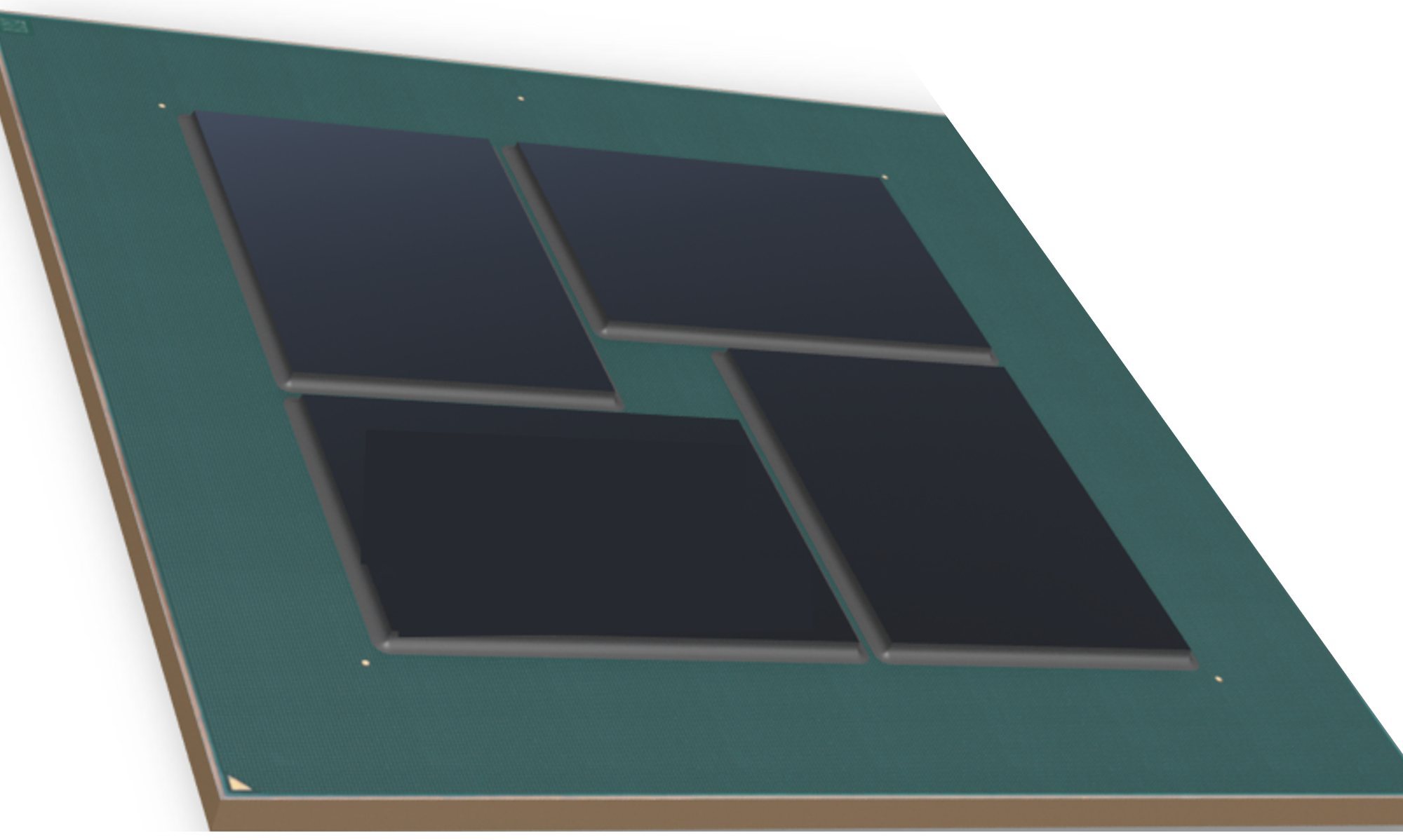
The design presented is a machine learning application fabricated in TSMC’s 12nm process. It consists of four die on an organic substrate (8/2/8). The package is an MCM FFCBGA (85 X 85) with 6,456 balls. The four-die system consumes 520 watts and is pictured above. By now, you should start to have a headache thinking about this design. I did. To complete the picture, each chip is a reticle size monster with 1.6B gates, 180MB of SRÅM and 204GB/s of memory bandwidth. Die-to-die communication is accomplished with an APLink 1.0 PHY. This design is truly a record-setting achievement, delivering 21.11 GFLOPS/watt.
Back to my headache. It got worse as James described the design challenges Alchip faced with this design. Soc design challenges include:
- >1B gate count and multiple level logical/physical hierarchy
- >100M on-chip SRAM and yield considerations
- Thousands of repeated cores and data bus traffic
- Extremely high static/dynamic power consumption and low power design
- Clock network design and power distribution network design
- DFT and testing strategy considering redundancy
For the package, design challenges include:
- Die-to-die interconnection on substrate
- PCB/package/SoC co-design
- Thermal considerations
- Warpage with 85x85mm² package size
Your head really has to be hurting at this point. So, how does one implement a design of this extreme complexity and size? Alchip packed a lot of innovation into the design process. James outlined some of the approaches. At the physical level, a channel-less floorplan with symmetry was used. The clocking strategy included chip-level clock phase control with a fishbone architecture. Power consumption was managed with adaptive voltage scaling, dynamic voltage and frequency scaling, clock and power gating, dual-rail SRAMs and a customized data path. In other words, just about every trick in the book, which is required to deliver reticle size designs and chiplet capabilities.
For DFT, an abutment design approach was used and custom DFT strategies were implemented for critical and non-critical logic. A redundancy and repair capability was also included. For testing and repair, the failure map was recorded in eFuse and the smart repair strategy considered scan and MBIST failures together.
Communication between the four dies is through the organic substrate as shown in the figure below. The APLink 1.0 PHY delivers 576Gbps per die-to-die channel in the N12 process. Multiple Tbps are possible in N7 and N5 and an APLink 3.0 design for 5nm technology is under development. The approach supports TSMC’s CoWoS and InFO packaging.

For signal integrity, 2.5D/3D model extraction was employed for high-speed signals and power-aware SPICE simulation accounted for noise induced effects. Power integrity required a lot of focus as each die draws over 150 amps of average current, with peak-to-peak variation greater than 40% of the average.
Given the high power of this design, electrical-thermal co-design was used and Alchip collaborated closely with the customer to model the cooling system. Mechanical samples were verified ahead of production to ensure warpage of the large interposer wouldn’t impact assembly yield.
This presentation was very impressive, and this design sets a new bar in complexity and power management. You can learn more about this reticle size design and its chiplet capabilities from Alchip’s press release.
Also Read:
Alchip moves from TSMC 7nm to 5nm!
Alchip Delivers Cutting Edge Design Support for Supercomputer Processor
CEO Interview: Johnny Shen of Alchip
Share this post via:


Comments
There are no comments yet.
You must register or log in to view/post comments.