

I attended the annual user group meeting called User2User in Santa Clara this year, hosted by Siemens EDA, with 51 presentations by customers in 11 tracks, and keynotes during each lunch hour from semiconductor executives. Joseph Sawicki, Executive VP, IC Segment, at Siemens EDA presented on a Tuesday, along with Prashant Varshney, Microsoft, and Mahesh Tirupattur, Analog Bits. This blog focuses on what I heard from Mr. Sawicki.
The host Harry Foster said that each keynote was like a Ted Talk, and they certainly lived up to that. Joseph’s topic was, From ICs to Systems – New Opportunities for the Semiconductor Industry. Digitalization is driving across all industries: Aerospace, auto, consumer, electronics and semi, energy, heavy, medical, marine, industrial.
There is now a pervasive AI enablement; in sensors, edge computing, 5G/wireless comm, cloud and data centers. The share of semiconductors in electronic systems from the time period of 1992- 2014 was 16%, but now has grown to about 24%, and predictions show that electronic systems will reach $3.2T revenue by 2025, so quite the growth market.
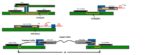
Systems companies are becoming IC designers, and there are many examples: Apple, Amazon, Google, ZTE, Tesla, Bosch, Huawei, Facebook. Foundries have seen the Systems companies grow from just 1% of revenue in 2011, now to 21% in 2021, that’s big growth and Apple has become the number one customer of TSMC. At the Hot Chips conference in 2006 just 16% of the accepted papers came from systems companies, while by 2021 that number had grown to 33% of the papers. So the systems companies are driving innovation in chip design.
Consider the history of Apple, their first 64 bit application processor was introduced way back in 2013, but why do that? Even in 2022 you still don’t need 64 bits for the larger RAM address space. The answer was for performance, an ARM core can run either in 32 or 64 bit modes, and running in 64 bit mode has 31% better performance.
There’s some new trends in automotive, Cars as a Service, where Volvo plans to reach 50% of their revenue through services by 2025. Tesla provides OTA (Over The Air) update services and new feature upgrades, adding revenue after the initial sales. Gartner Group reports that half of the top 10 auto OEMS will be designing some of their own chips by 2025, with 7 of 10 already announced by 2021. Ford and Globalfoundries will partner in IC design in order to smooth out the supply chain issues that have hurt the industry since the COVID pandemic started in 2020.
The gradual electrification of vehicles is a major driver of new IC design starts, and the semiconductor revenue per vehicle should reach $500 per car by 2028, so that’s a $24B market. 5G communication will be important to automotive for OTA updates and services, and is growing 3X per year.
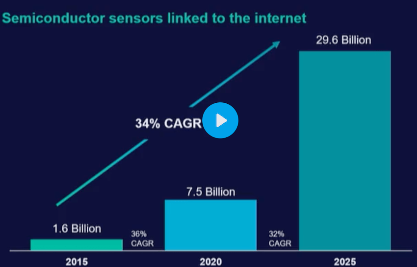
The total number of sensors connected to Internet was 1.6B in 2015, exploding in growth to 29.6B sensors by 2025, so that’s big growth of video, data, and data center.
Semiconductor content inside of Data Centers is growing to $242B by 2030, which is a 14% CAGR, per IBS, Sept. 2021.
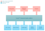
With all of these demands on semiconductors in growth markets, how is our industry going to meet the them? Joseph summarized that there are three trends to meet demand:
- Technology scaling – new nodes and 3D IC
- Design scaling – silicon integration
- System scaling – digital twin, verifying a device against spec and the full SW stack with apps
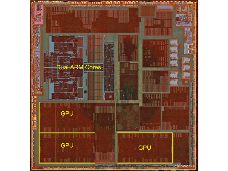
For technology scaling we can look at Moore’s Law, it’s not quite dead, because look at the A-series from Apple over time. From 2013 to 2021, we saw transistor counts growing from 1 billion to 15 billion, so it’s still scaling pretty well at 15X. Dennard Scaling has died – so clock cycle rates are not improving by 16X over that 8 year time frame. Looking at single core CPU performance , the Geekbench scores have ranged from 269 to 1734, so it’s growing on track. Even the foundries have another 8 years to grow process technology in their road maps.
Monolithic integration is growing, yes, but 3D design is coming along too, combined with innovative packaging. System in a Package is a new trend. System and design technology co-optimization is needed to be successful.
On design scaling there are charts that claim that 7nm designs cost $280M, but is that reality? That number sounds too big, yet the trend line is true, as small nodes drive up the design and verification costs. One method to counter that increase in costs is to move from RTL up to C level design for systems designs. Consider the example of NVIDIA, where a small team of just 10 engineers in 6 months taped out a new chip for deep learning inference accelerator by using C++ with an HLS (High Level Synthesis) methodology, as reported at Hot Chips in Aug 2019. Google is another systems company using HLS to help manage SoC design costs.
For System Scaling the idea is to create a true digital twin. One example of digital twin is something called PAVE360 – it’s a way to validate automotive models with traffic, people and vehicles. You can run this digital twin in order to validate virtual models, or run SW for your ADAS system, to model power, vehicle modeling (power train, chassis, seating, effect of road on occupants). It’s a way to safely validate before production starts.
The final topic was lifecycle management, so consider a data center with hundreds of thousands of blades, where you can actually monitor all of the blades in real time, debug any reliability issues in that data center, and you can analyze all of the embedded sensor data, literally tracking the health of the data center.
Summary
A trillion dollar semiconductor industry is shortly approaching us, so this is an exciting time to be part of the EDA industry which enables all of this growth, as systems designers are taking on new design starts, AI is everywhere, electrification of vehicles continues, and digital twins are being adopted. The mood of the presentation was quite upbeat, and well received by the audience.


