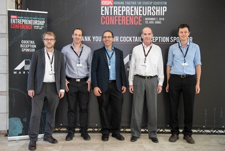
Dr. Robert Giterman is Co-Founder and CEO of RAAAM Memory Technologies Ltd, and has over nine-years of experience with the research and development of GCRAM technology, which is being commercialized by RAAAM. Dr. Giterman obtained his PhD from the Emerging Nanoscaled Circuits and Systems Labs Research Center in Bar-Ilan University. Following the completion of his PhD in 2018, he joined the Telecommunications Circuits Laboratory in the Ecole Polytechnique Federale de Lausanne, Switzerland, as a post-doctoral researcher. As part of his research, he has led the front-end and physical implementations of multiple ASICs, and mentored numerous PhD thesis and MSc projects in the field of VLSI embedded memories. Dr. Giterman has authored over 40 scientific papers and holds 10 patents.
First, please tell me about RAAAM?
RAAAM Memory Technologies Ltd. is an innovative embedded memory solutions provider, that delivers the most cost-effective on-chip memory technology in the semiconductor industry. RAAAM’s silicon-proven Gain-Cell RAM (GCRAM) technology combines the density advantages of embedded DRAM with SRAM performance, without any modifications to the standard CMOS process available from multiple foundries.
RAAAM’s patented GCRAM technology can be used by semiconductor companies as a drop-in replacement for SRAM in their SoCs, allowing to significantly reduce fabrication costs through a significant die size reduction. Alternatively, increasing the on-chip memory capacity in the same die size enables a dramatic reduction in the off-chip data movement to resolve the memory bottleneck. This increase in on-chip memory capacity will enable additional features that can enable industry growth for applications in the areas of AR/VR, Machine Learning (ML), Internet-of-Things (IoT), and Automotive.
What problem are you solving?
Important industry growth drivers, such as ML, IoT, Automotive and AR/VR, operate on ever-growing amounts of data that is typically stored off-chip in an external DRAM. Unfortunately, off-chip memory accesses are up-to 1000x more costly in latency and power compared to on-chip data movement. This limits the bandwidth and power efficiency of modern systems. In order to reduce these off-chip data movements, almost all SoCs incorporate large amounts of on-chip embedded memory caches that are typically implemented with SRAM and often constitute over 50% of the silicon area. This memory bottleneck is further aggravated since SRAM scaling has been increasingly difficult in recent nodes, shrinking only at a rate of 20%-25% compared to almost 50% scaling for logic.
Can you tell us more about GCRAM technology?
GCRAM technology relies on a high-density bitcell that requires only 2-3 transistors (depending on priorities on area or performance). This structure offers up-to 2X area reduction over high-density 6T SRAM designs. The bitcell is composed of decoupled write and read ports, providing native two ported operation, with a parasitic storage node capacitor keeping the data. Unlike conventional 1T-1C eDRAM, GCRAM does not rely on delicate charge sharing to read the data. Instead, our GCRAM provides an active read transistor that provides an amplified bit-line current, offering low-latency non-destructive readout without the need for large storage capacitors. As a result, GCRAM does not require any changes or additional costs to the standard CMOS fabrication process and scales with technology when properly designed.
While the concept of 2T/3T memory cells has been tried in the past, reduction of the parasitic storage capacitor and concerns about increasing leakage currents has so far discouraged its application beyond 65nm. RAAAM’s patented innovations comprise clever circuit design at both memory bitcell and periphery levels, resulting in significantly reduced bitcell leakage and enhanced data retention times, as well as specialized refresh algorithms optimized for various applications, ensuring very high memory availability even under the most extreme operating conditions. In fact, we had demonstrated the successful scaling of GCRAM technology across process nodes of various foundries (e.g., TSMC, ST, Samsung, UMC), including recent silicon demonstrators in 28nm (Bulk and FD-SOI) and 16nm FinFET technologies implementing up-to 1Mbit of GCRAM memory macros.
Can you share details about your team at RAAAM and what has been done to validate the GCRAM technology?
RAAAM founders, including Robert Giterman, Andreas Burg, Alexander Fish, Adam Teman and Danny Biran, bring over 100+ combined years of semiconductor experience. In fact, RAAAM is built on a decade of world-leading research in the area of embedded memories, and GCRAM in particular. Our work on GCRAM technology has been demonstrated on 10 silicon prototypes of leading semiconductor foundries in a wide range of process nodes ranging from 16nm to 180nm, including bulk CMOS, FD-SOI and FinFET processes. Our work on GCRAM is documented by more than 30 peer-reviewed scientific publications in books, journals, and conference proceedings, and is protected by 10 patents.
Who is going to use RAAAM’s technology and what will they gain?
RAAAM’s GCRAM technology enables a significant chip fabrication cost reduction or highly improved performance, resolving the memory bottleneck for semiconductor companies in various application fields. Since GCRAM is directly compatible with any standard CMOS process and uses an SRAM-like interface, it can easily be integrated into existing SoC designs.
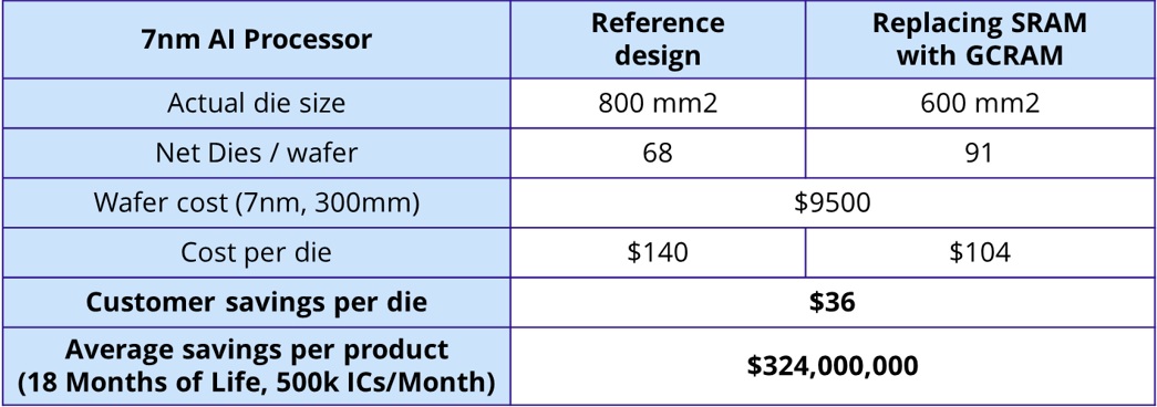
As an example for potential system benefits, we can look at the Machine Learning accelerators domain using a 7nm AI processor integrating 900MB of SRAM on a single die. In this case, the SRAM area constitutes over 50% of the overall die size. Replacing SRAM with RAAAM’s GCRAM technology can provide a reduction of up-to 25% of the overall die size, resulting in up-to $35 savings per die.

Alternatively, for memory-bandwidth limited systems, increasing the on-chip memory capacity can bring substantial performance and power improvements. In fact, the required DRAM bandwidth is often inversely proportional to the on-chip memory capacity. With off-chip memory accesses being up-to 1000x more costly in power and latency compared to on-chip data movement, replacing SRAM with 2X more GCRAM capacity at the same area footprint significantly reduces the off-chip bandwidth requirements and enables RAAAM’s customers to gain a competitive advantage in the power consumption of their chip.
What is RAAAM’s engagement model?
RAAAM follows an IP vendor licensing model. Semiconductor companies can license RAAAM’s GCRAM technology for a fee and production unit royalties RAAAM implements the front-end memory controller and GCRAM-based hard memory macros according to the customer specifications and delivers a soft RTL wrapper (using a standard SRAM interface), which instantiates the GCRAM hard
macros (GDS) and the soft refresh control (RTL). Additionally, the customer receives a characterization report of the hard memory macro and a behavioral model for system-level verification. At present,
RAAAM is working on the implementation and qualification of a GCRAM-based memory compiler, which will enable RAAAM’s customers to automatically generate the complete front and back-end views of GCRAM IP and corresponding characterization reports according to customer specifications.
Can you tell us about your recent achievements?
RAAAM has made very exciting progress recently. First, we have been evaluating the benefits of our technology for leading semiconductor companies, which has confirmed our projected substantial improvements from a performance and cost perspective over existing solutions based on SRAM. In fact, we have recently engaged with a very large semiconductor company on a long-term, co-development project and we continue running customer evaluations for various application fields and process nodes. We see growing interest in our technology in a variety of applications, both in very advanced process (7nm and beyond) nodes and in less advanced ones (16nm and higher). Finally, we are extremely pleased to have joined the Silicon Catalyst Incubator, allowing us to gain access to their comprehensive ecosystem of In-Kind Partners, Advisors, and Corporate VC and institutional investor network.
What is on the horizon for RAAAM?
Our product development roadmap includes full memory qualification in selected nodes of leading semiconductor foundries, based on customer demand. In addition, we have on-going discussions with numerous foundries for further technology migration to their next generation process nodes. Furthermore, we are looking to expand our embedded memory platform and introduce design flow automation based on our memory compiler development efforts. To this end, we are in the process of raising Seed funding to fully qualify our GCRAM technology and to accelerate our company’s overall business growth.
A preliminary GCRAM product brief is available upon request, please send an email to info@raaam-tech.com. Additional information can be found at: https://raaam-tech.com/technology https://www.linkedin.com/company/raaam
Also read:
CEO Interview: Dr. Esko Mikkola of Alphacore
CEO Interview: Kelly Peng of Kura Technologies
CEO Interview: Aki Fujimura of D2S
Share this post via:


Is Intel About to Take Flight?