My first exposure to seeing multiple die inside of a single package in order to get greater storage was way back in 1978 at Intel, when they combined two 4K bit DRAM die in one package, creating an 8K DRAM chip, called the 2109. Even Apple used two 16K bit DRAM chips from Mostek to form a 32K bit DRAM, included in the Apple III computer, circa 1978. So the concept to assemble multiple die into a single package has been around for decades now. The new name for this methodology is System Technology Co-Optimization, or STCO for short, because system-level engineers are now combing memory, processors, mixed-signal IP and sensors into single packages.
Some electronic systems can be built on a single SoC economically, while other system approaches are using packaging techniques in order to interconnect multiple, specialized die, yielding lower costs than a monolithic approach. With multiple die involved, there is a new challenge in how to optimize such a system.
Per Viklund at Siemens EDA wrote a white paper on this topic, and I’ll share the highlights in this blog. Chiplets are being used to save costs over a single SoC implementation, and the interconnect is through High Density Advanced Packaging (HDAP) approaches with 2.5D and 3D stacked die. Prototyping is recommended for STCO success, to ensure that the effects of power integrity, signal integrity, thermal, warp and mechanical stress are understood before production begins.

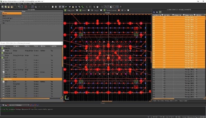
Waiting for all of the chiplets to be designed, and then starting the packaging design process is much too late in the schedule to make any partitioning trade-offs, so the preferred approach is to start the package design quite early as a package prototype. The idea is to iterate on several alternative package prototypes when it’s possible to impact the partitioning of features into each chiplet. At the earliest stage of package prototype there may be few details per chiplet, but the idea is to incrementally add more information.
Even with a package prototype it’s possible to run early analysis of power integrity and signal integrity. An early model has approximate chiplet sizes and the interconnect signals, so using power integrity tools an engineer can determine how many power and ground bumps are needed for the package as a first pass to spot any issues.

With the package prototype methodology it’s possible to run early simulations to uncover and fix issues with mechanical stress, warping, die attachment and metal cracking. As each chiplet is completed, then more detailed analysis can replace the earlier prototype results. There’s also a final, 3D fully assembly verification, to make certain that there are no surprises.
Summary
There is a methodology for System Technology Co-Optimization (STCO), applied to chiplet-based designs, which involves creating a prototype package early in the system design process, then running early analysis, and to start making partitioning trade-offs. Physical effects are considered early in the prototyping process, and multi-physics analysis finds and fixes any issues.
This is another example of shift left, applied to system projects using HDAP. To read the complete, seven page White Paper, Using a System Technology Co-Optimization (STCO) Approach for 2.5/3D Heterogeneous Semiconductor Integration, visit the Siemens EDA site, and provide some basic information to download.
Related Blogs
- Heterogeneous Package Design Challenges for ADAS
- From Silicon To Systems
- Heterogeneous Chiplets Design and Integration


Comments
There are no comments yet.
You must register or log in to view/post comments.