TSMC recently held their annual Technology Symposium in Santa Clara, CA. The presentations provided a comprehensive overview of their status and upcoming roadmap, covering all facets of process technology and advanced packaging development. This article will summarize the highlights of the process technology updates – a subsequent article will cover the advanced packaging area.
First, here is a brief overview of some of the general observations and broader industry trends, as reported by C.C. Wei, TSMC CEO.
General
- “This year marks TSMC’s 35th anniversary. In 1987, we had 258 employees in one location, and released 28 products across 3 technologies. Ten years later, we had 5,600 employees, and released 915 products across 20 technologies. This year in 2022, we have 63,000 employees, and will release 12,000 products across 300 technologies.”
- “From 2018 to 2022, the volume of 12” (equivalent) wafers has had an annual CAGR exceeding 70%. In particular, we are seeing a significant increase in the number of ‘big die’ products.” (>500mm**2)
- “In 2021, TSMC’s North America business segment shipped more than 7M wafers and over 5,500 products. There were 700 new products tapeouts (NTOs). This segment represents 65% of TSMC’s revenue.”
- “Our gigafab expansion plans have typically involved adding two new ‘phases’ each year – that was the case from 2017-2019. In 2020, we opened six new phases, including our advanced packaging fab. In 2021, there were seven new phases, including fabs in Taiwan and overseas – advanced packaging capacity was added, as well. In 2022, there will be 5 new phases, both in Taiwan and overseas.”
- N2 fabrication: Fab20 in Hsinchu
- N3: Fab 18 in Tainan
- N7 and N28: Fab22 in Kaohsiung
- N28: Fab16 in Nanjing China
- N16, N28, and specialty technologies: Fab23 in Kumanoto Japan (in 2024)
- N5 in Arizona (in 2024)
- “TSMC has 55% of the worldwide installed base of EUV lithography systems.”
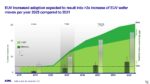
- “We are expanding our capital equipment investment significantly in 2022.” (The table below highlights the considerable jump in cap equipment planned expenditures.)
- “We are experiencing stress in the manufacturing capacity of mature process nodes. In 35 years, we have never increased the capacity of a mature node after a subsequent node has ramped to high volume manufacturing – that is changing.”
- “We continue to invest heavily in “intelligent manufacturing”, focusing on precision process control, tool productivity, and quality. Each gigafab handles 10M dispatch orders per day, and optimizes tool productivity. Each gigafab generates 70B data points daily to actively monitor.”
For the first time at the Symposium, a special “Innovation Zone” on the exhibit floor was allocated. The recent product offerings from a number of start-up companies were highlighted. TSMC indicated, “We have increased our support investment to assist small companies adopt our technologies. There is a dedicated team that focuses on start-ups. Support for smaller customers has always been a focus. Perhaps somewhere in this area will be the next Nvidia.”
Process Technology Review
With a couple of exceptions discussed further on, the process technology roadmap presentations were somewhat routine – that’s not a bad thing, but rather an indication of ongoing successful execution of prior roadmaps.
The roadmap updates were presented twice, once as part of the technology agenda, and again as part of TSMC’s focus on platform solutions. Recall that TSMC has specifically identified four “platforms” that individually receive development investment to optimize the process technology offerings: mobile; high-performance computing (HPC); automotive; and IoT (ultra-low power). The summaries below merge the two presentations.
N7/N6
- over 400 NTOs by year-end 2022, primarily in the smartphone and CPU markets
- N6 offers transparent migration from N7, enabling IP re-use
- N6RF will be the RF solution for upcoming WiFi7 products
- there is an N7HPC variant (not shown in the figure above), providing ~10% performance improvement at overdrive VDD levels
For N6, logic cell-based blocks can be re-implemented in a new library for additional performance improvements, achieving a major logic density improvement (~18%).
N5/N4
- in the 3rd year of production, with over 2M wafers shipped, 150 NTOs by year-end 2022
- mobile customers were the first, followed by HPC products
- roadmap includes ongoing N4 process enhancements
- N4P foundation IP is ready, interface IP available in 3Q2022 (to the v1.0 PDK)
- there is an N5HPC variant (not shown in the figure above, ~8% perf improvement, HVM in 2H22)
As with the N7/N6, N4 provides “design re-use” compatibility with N5 hard IP, with a cell-based block re-implementation option.
The complexity of SoC designs for the automotive segment is accelerating. There will be an N5A process variant for the automotive platform, qualified to AEC-Q100 Grade 1 environmental and reliability targets (target date: 2H22). The N5A automotive process qualification involves both modeling and analysis updates (e.g., device aging models, thermal-aware electromigration analysis).
N3 and N3E
- N3 will be in HVM starting in the second half of 2022
- N3E process variant in HVM one year later; TSMC is expecting broad adoption across mobile and HPC platforms
- N3E is ready for design start (v0.9 PDK), with high yield on the standard 256Mb memory array qualification testsite
- N3E adds the “FinFLEX” methodology option, with three different cell libraries optimized for different PPA requirements (more at the end of this article)
Note that N3 and N3E are somewhat of an anomaly to the prior TSMC process roadmap. N3E will not offer a transparent migration of IP from N3. The N3E offering is a bit of a “correction”, in that significant design rule changes to N3 were adopted to improve yield.
TSMC’s early-adopter customers push for process PPA updates on an aggressive timeline, whether an incremental, compatible variant to an existing baseline (e.g., N7 to N6, N5 to N4), or for a new node. The original N3 process definition has a good pipeline of NTOs, but N3E will be the foundation for future variants.
N2
- based on a nanosheet technology, target production date: 2025
- compared to N3E, N2 will offer ~10-15% performance improvement (@iso-power, 0.75V) or ~25-30% power reduction (@iso-perf, 0.75V); note also the specified operating range in the figure above down to 0.55V
- N2 will offer support for a backside power distribution network
Parenthetically, TSMC is faced with the dilemma that the requirements of the different platforms have such a broad range of targets for power, performance, and area/cost. As was noted above, N3E is addressing these targets with different libraries, incorporating a different number of fins that define the cell height. For N2 library design, this design decision is replaced by a process technology decision on the number of vertically-stacked nanosheets throughout (with some allowed variation in the device nanosheet width). It will be interesting to see what TSMC chooses to offer for N2 to cover the mobile and HPC markets, in terms of the nanosheet topology. (The image below from an earlier TSMC technical presentation at the VLSI 2022 Conference depicts 3 nanosheets.)
NB: There are two emerging process technologies being pursued to reduce power delivery impedance and improve local routability – i.e., “buried” power rail (BPR) and “backside” power distribution (BSPDN). The initial investigations into offering BPR have quickly expanded to process roadmaps that integrate full BSPDN, like N2. Yet, it is easy to get the two acronyms confused.
Specialty Technologies
TSMC defines the following offerings into a class denoted as “specialty technologies”:
- ultra-low power/ultra-low leakage (utilizing an ultra-high Vt device variant)
- requires specific focus on ultra-low leakage SRAM bitcell design
- N12e in production, N6e in development (focus on very low VDD model support)
- (embedded) non-volatile memory
- usually integrated with a microcontroller (MCU), typically in a ULP/ULL process
- RRAM
- requires 2 additional masks, embedded in BEOL (much lower cost than the 12 masks for eFlash)
- 10K write cycles (endurance specification), ~10 years retention @125C
-
- MRAM
- 22MRAM in production, focus is on improving endurance
- 16MRAM for Automotive Grade 1 applications in 2023
- power management ICs (PMIC)
- based on bipolar-CMOS-DMOS (BCD) devices: 40BCD+, 22BCD+
- for complex 48V/12V power domains
- requires extremely low device R_on
- high voltage applications (e.g., display drivers, using N80HV or N55HV)
- analog/mixed-signal applications, requiring unique active and passive structures (e.g., precision thin-film resistors and low noise devices, using N22ULL and N16FFC)
- MEMS (used in motion sensors, pressure sensors)
- CMOS image sensors (CIS)
- pixel size of 1.75um in N65, 0.5um in N28, transitioning to N12FFC
- radio frequency (RF), spanning from mmWave to longer wavelength wireless communication; the upcoming WiFi7 standard was highlighted
“The transition from WiFi6 to WiFi7 will require a significant increase in area and power, to support the increased bandwidth requirements – e.g., 2.2X area and 2.1X power. TSMC is qualifying the N6RF offering, with a ~30-40% power reduction compared to N16RF. This will allow customers currently using N16RF to roughly maintain existing power/area targets, when developing WiFi7 designs.”
The charts below illustrate how these specialty technologies are a fundamental part of platform products – e.g., smartphones and automotive products. The characteristic process nodes used for these applications are also shown.
Although the focus of smartphone development tends to be on the main application processor, the chart below highlights the extremely diverse requirements for specialty technology offerings, and their related features. In the automotive area, the transition to a “zonal control” architecture will require a new set of automotive ICs.
N3E and FinFLEX
The FinFLEX methodology announcement was emphasized, with TSMC indicating “FinFLEX will offer full-node scaling from N5.”
As FinFET technology nodes have scaled – i.e., from N16 to N10 to N7 to N5 – the fin profile and drive current_per_micron have improved significantly. Standard cell library design has evolved to incorporating fewer pFET and nFET fins that define the cell height (specified in terms of the number of horizontal metal routing tracks). As illustrated above, the N5 library used a 2-2 fin definition – that is, 2 pFET fins and 2 nFET fins to define the cell height. (N16/N12 used a 3-3 configuration.)
The library definition for N3E was faced with a couple of issues. Mobile and HPC platform applications are increasingly divergent, in terms of their PPA (and cost) goals. Mobile products focus on circuit density to integrate more functionality and/or reduced power, with less demanding performance improvements. HPC is much more focused on maximizing performance.
As a result, N3E will offer three libraries, as depicted in the figure above:
-
- an ultra low power library (cell height based on a 1-fin library)
- an efficient library (cell height based on a 2-fin library)
- a performance library (cell height based on a 3-fin library)
The figure below is from TSMC’s FinFLEX web site, illustrating the concept (link).
Now, offering multiple libraries for integration on a single SoC is not new. For years, processor companies have developed unique “datapath” and “control logic” library offerings, with different targets for: cell heights, circuit performance, routability (i.e., max cell area utilization), and distinct logic offerings (e.g., wide AND-OR gates for datapath multiplexing). Yet, the physical implementation of SoC designs using multiple libraries relied upon a consistent library per design block.
The unique nature of the FinFLEX methodology is that multiple libraries and multiple track heights will be intermixed within a block.
After the TSMC Symposium, additional information became available. A block design will alternate rows for the two libraries. For example, a 3:2 block design will have alternate row heights accommodating cells from the 3-fin and 2-fin library designs. A 2:1 block design will have alternate rows for cells from the 2-fin and 1-fin libraries.
TSMC indicated, “Different cell heights (in separate rows) are enabled in one block to optimize PPA. FinFLEX in N3E incorporates new design rules, new layout techniques, and significant changes to EDA implementation flows.”
There will certainly be more information to come about FinFLEX and the changes to the general design flow. Off-hand, there will need to be new approaches to:
-
- physical synthesis
- how will synthesis improve timing on a critical signal
- will synthesis strive to provide a netlist with a balanced ratio of cells from the two libraries for the alternating rows
For example, to improve timing on a highly-loaded signal, synthesis would typically update a cell assignment in the library to the next higher drive strength – e.g., NAND2_1X to NAND2_2X.
With FinFLEX, additional options are available with the second library – e.g., whether an update to NAND2_1X_2fin would use NAND2_2X_2fin or NAND2_1X_3fin. Yet, if the latter is chosen, the new cell will need to be “re-balanced” to a different row in the block floorplan. The effective changes in performance and input/output wire loading for these choices are potentially quite complex to estimate during physical synthesis.
The cell selection options get even more intricate when considering specific flop cells to use, given not only the differences in clock-to-Q delays, but also the setup and hold time characteristics, and input clock loading. When would it be better for individual flop bits in a register to use different output drive strengths in the same library (and be placed locally) versus having register bits re-balanced to a row corresponding to a different library selection?
With an alternating row configuration, the assumption is that there will be an even mix of cells from the two libraries. Yet, the synthesis of a block may only require a small percentage of “high-performance” cells to meet timing objectives. An output netlist without a balanced mix of library cells may have low overall utilization, suggesting a uniform row, single-library block floorplan may be suitable instead. This may result in iterations in the chip floorplan (and likely, revisions in the power distribution network, as well).
-
- sub-block level IP integration
Blocks often contain a number of small hard IP macros, such as register files (typically provided by a register file generator). With non-uniform row heights, the algorithms in the generator become more complex, to align the power continuity between the macro circuits and the cell rows. And, there will be placement restriction rules that will need to be added to the hard IP models.
-
- timing/power optimizations during physical design
Similarly to the physical synthesis block construction options, there will be difficult decisions on cell selection during the timing and power optimization steps in the physical design flow. For example, if a cell can reduce its assigned drive strength to save power while still meeting timing, would a change in library selection, and thus row re-balancing, be considered? Would the corresponding changes in the cell placement negate the optimization?
and, last but most certainly not least,
-
- Will there be new EDA license costs to enable N3E FinFLEX?
(Years ago, the CAD department manager at a previous employer of mine went viral at the license cost adder to enable placement and routing for multipatterning requirements. Given the significant EDA investment required to support FinFLEX, history may repeat itself with additional license feature costs.)
The FinFLEX methodology definitely offers some intriguing options. It will be extremely interesting to see how this approach evolves.
Analog design migration automation
Lastly, TSMC briefly highlighted work they are pursuing in the area of assisting designers migrate analog/mixed-signal circuits and layouts to newer process nodes.
Specifically, TSMC has defined a set of “analog cells”, with the capability to take an existing schematic, re-map to a new node, evaluate circuit optimizations, and migrate layouts, including auto-placement and (PG + signal) routing.
The definition of the analog cell libraries for N5/N4 and N3E are complete, with N7/N6 support to follow. TSMC showed an example of an operational transconductance amplifier (OTA) that had been through the migration flow.
Look for more details to follow. (This initiative appears to overlap with comparable features available from EDA vendor custom physical design platforms.)
A subsequent article will cover TSMC’s advanced packaging announcements at the 2022 Technology Symposium.
-chipguy
Also read:
Three Key Takeaways from the 2022 TSMC Technical Symposium!
Inverse Lithography Technology – A Status Update from TSMC
TSMC N3 will be a Record Setting Node!


