
SemiWiki recently posted a blog on “Deep Data Analytics for Accelerating SoC Product Development.” That blog focused on proteanTecs’ AI-enabled chip analytics platform that helps accelerate SoC product development. The blog provided insight into proteanTecs’ approach and shared quantifiable business-impact metrics as derived by Semico using a sample data center accelerator SoC.
proteanTecs recently published a whitepaper on how to enhance the economics of testing by leveraging its solution together with Advantest’s Advanced Cloud Solutions (ACS) Edge solution. With proteanTecs delivering enhanced visibility through embedded Universal Chip Telemetry (UCT), the ACS Edge enables the production test environment for real-time execution. The combination elevates production testing to a new level. This post will discuss the salient points garnered from that whitepaper.
Challenges for Enhanced Testing
With the ever increasing levels of system integration, the following are some of the Testing challenges.
-
- Applications involve increasing amounts of hardware-software interactions, whether it is mobile oriented products or other embedded products
- Ever increasing levels of integration within the same physical constraint makes it hard to understand the operating conditions at failure
- Difficulty correlating results across test, assembly and system integration stages, due to lack of a common data language
- Lack of visibility into operating conditions leading up to a failure, thereby making root cause analysis (RCA) difficult
Gaps in Current Testing Approaches
Traditionally, each stage of testing from post-silicon validation to system level testing has been with different equipment using different data languages for describing the respective tests. While the segmented approach may have helped optimize each stage, overall results could fall short of what is achievable through an integrated approach. As the segmented approach lacks data sharing among different testing stages, optimizing product cost is difficult. An overall optimization workflow with data sharing is needed for effective and economically efficient testing.
Moving Coverage Between Stages
Wafer Test has the highest cost per second, followed by Package Test and then System Level Test (SLT). But in order for a device manufacturer to guarantee the field failure rate, all that matters is the quality and reliability of the final product. As a device moves through different stages, the test cost vs cost of scrapping a device changes, directly impacting the profitability of a product. Naturally, a device manufacturer would want to run all of the effective screens at the earliest point, saving only elusive faults for system level testing.
For example, $500K of scrap costs may have been avoided by moving 5% coverage from package test to wafer sort. In order to shift-left or shift-right some coverage, one must correlate if the test at one stage is equivalent to the test at another stage. But that decision to move can only be enabled through improved visibility into each stage, allowing tests to be adjusted for each test insertion.
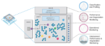
proteanTecs Platform
proteanTecs platform is designed to provide detailed device visibility from initial manufacturing testing throughout the device’s lifetime. It is a holistic software platform that applies machine learning and analytics to data created by on-chip UCT agents. The platform’s pre-configured set of dashboards provide meaningful and useful insights and alerts. The platform is scalable and flexible and fuses information from the entire fleet of chips and systems. And, it offers an open development environment for incorporation of customized algorithms.
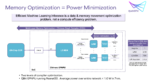
Advantest’s ACS Edge™ Platform
Advantest’s ACS Edge™ is a high performance, highly secure edge compute and analytics solution enabling ultra-fast algorithmic AI decision making with millisecond latencies during test execution. ACS Edge connects to test equipment via a private high-speed encrypted link. Users develop machine learning or other compute-intensive applications which operate near real-time on data generated by tests in the test program. These applications are wrapped in an Open Container Initiative (OCI) compliant container which simplifies global distribution and management while hardening them against compute environment changes.
proteanTecs + ACS Edge: Tremendous Potential
The combination of the proteanTecs analytics platform with the ACS Edge analytics solution offers tremendous potential to change the economics of testing. Compared to traditional testing approaches, the combined solution delivers the following benefits.
-
- Reduced test execution time (more than 70% reduction compared to traditional approaches)
- Production yield improvement (more than 2% compared to traditional approaches)
- Enhanced outlier detection within an insertion
- Real-time adaptive test
- Reduction in retesting
- Improved visibility for shift-left decisions
The whitepaper includes lot of examples and use cases with benefits achieved reported in quantified form. For full details, download the joint whitepaper.
For more details about:
The proteanTecs platform, visit https://www.proteantecs.com/solutions
The ACS Edge platform, visit https://www.advantest.com/acs/edge
Also Read:
proteanTecs Technology Helps GUC Characterize Its GLink™ High-Speed Interface


