A recent SemiWiki post covered the topic of protecting high-speed interfaces in data centers using security IP. That post was based on a presentation made by Dana Neustadter at IP-Soc Silicon Valley 2022 conference. Dana’s talk was an overview of various interfaces and Synopsys’ security IP for protecting those interfaces. As a senior product marketing manager for Security IP, Dana has now written a technical bulletin that dives into the details of memory security. This post is based on a review of that bulletin.
Technology – A Double-Edged Sword
Many of us have seen (or heard of) the Steven Spielberg movie “Catch Me If You Can” starring Leonardo DiCaprio. The movie is based on the real life of Frank Abagnale who turned into a con artist at a very young age. While the movie may have taken some Hollywood liberties, it is true that Frank committed lots of crimes until he was caught and served time. His crimes included simple things such as writing fraudulent checks, to impersonating an airline pilot and even a resident doctor. After serving time, he reformed and has been serving the FBI for many decades, helping prevent white-collar crimes and/or catching criminals.
A few years ago, Frank Abagnale appeared on the Google Tech Talks series and gave a talk to a technology audience. An audience member asked Frank if he felt he would be able to successfully commit all the crimes in the current technology era. To the audience’s surprise, Frank said it is much easier now than it was four decades ago. Frank went on to explain that while technology offers more things, faster, cheaper and easier to use, these aspects also make it easier for a smart criminal.
The technology world’s challenge is to offer security solutions that work seamlessly with advanced products without compromising on performance, ease of use and flexibility among other requirements. Factors such as laws and regulations, changing nature of security threats, a growing attack surface and standards evolution are all placing the spotlight on security solutions.
Encryption at the Heart of Memory Security
Preventing security breaches involves many steps, but encryption is always at the heart of the solution. If data is encrypted, even if someone gets their hands on the data, they cannot do malicious things using the encrypted data. While security solutions need to be hard to break, it is also critical for the encryption/decryption process to be quick and easy. Naturally, encryption algorithms have been getting a lot of attention over the decades.
Characteristics of a Good Memory Security Solution
A good memory security solution needs to support not only the latest interfaces but also utilize minimal additional chip/board real estate and execute with very low latency. AES-XTS, or as it is sometimes referred XTS-AES, is the de-facto cryptographic algorithm for protecting the confidentiality of data-at-rest and in-use on storage devices.
It is a standards-based symmetric algorithm defined by NIST SP800-38E and IEEE Std 1619-2018 specifications. By design, it allows for pipelined architectures that can scale in performance to Terabits per second (Tbps) bandwidth. And its Ciphertext Stealing (CTS) mode provides support for data units with sizes that are not divisible by the 16-byte block size of the underlying AES cipher.
While it is one thing to have a standardized algorithm, it is yet another thing to deploy an optimized implementation of the same algorithm. The implementation needs to not only use minimal area and work at low latency but also support all key sizes and seamless context switching for a high number of changing contexts. And in particular for deployments in North America, the implementation should be certifiable to at least FIPS 140-3 Level 2, if not Level 3 for more security sensitive applications.
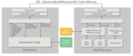
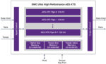
Synopsys’s Ultra High-Performance AES-XTS IP for HPC
Synopsys Ultra High-Performance AES-XTS Cryptographic IP core (see block diagram below) possesses the above characteristics while providing the flexibility needed to adjust to SoC designs’ specific use cases.
Some key benefits of integrating Synopsys’ standards-compliant AES-XTS crypto cores include:
- High performance, low latency IP with efficient support for varied data traffic
- Scalable throughput from 128 to 4096 bits/cycle, achieving bandwidths beyond 4 Tbps
- Efficient encryption and decryption with 256-bit and 512-bit AES-XTS key sizes
- Latency as low as 4 cycles
- One tweak per cycle pre-computation
- Seamless message interleaving, key setup, and key refresh for up to 64K cryptographic contexts
- Multi-clock domain support
- Dedicated secure key port
- Area, latency, performance, and maximum frequency optimization options
- FIPS 140-3 certification ready
- Path for seamless full-duplex inline memory encryption integration with memory interface controllers
- Support for the latest memory interfaces generations DDR4/LPDDR4 and DDR5/LPDDR5
Click here for accessing the whole technical bulletin. Synopsys offers a number of highly configurable security IP solutions. For more details, refer to the security IP product page.