
Product LifeCycle Management (PLM) systems have shown incredible value for integrating the enterprise with a single view of the product design, deployment, maintenance, and end-of-life processes. PLM systems have traditionally grown from the mechanical design space, and this still forms their strength.
Meanwhile, due to the revolution in semiconductors, electronics systems have become increasingly integrated within system designs in nearly all industrial segments. To date, PLM systems have handled electronics systems largely as pseudo-mechanical components. However, with the rapid increase in electronic value (example: over 40% of automotive cost), this treatment of electronics within PLM systems is breaking down the fundamental value of PLM for their customers. This article outlines the increasing gaps created by electronics in PLM systems, and the nature of the required solutions.
What is the value of PLM?
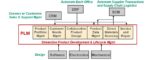
Figure 1: PLM
Most product development teams use PLM systems from companies such as PTC, Siemens, Dassault, Zuken, Aras and others to integrate major functions of the enterprise (figure one). Underlying technologies of data vaulting, structured workflows, collaboration, and analytics provide a coherent view of the state of a project and the significant value delivered is a streamlined product development and lifecycle management capability. PLM infrastructure intersects with design through domain specific design tools (mechanical, electronic, software, and more). The semantic understanding of any underlying data held by PLM is actually contained in these domain specific design tools. All the significant parts of the enterprise (design, manufacturing, field, product definition) use these design domain specific tools to interact with the underlying PLM data.
System PCB Electronic Design:
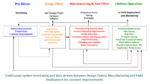
Figure 2: Electronics Design Process for System PCB customers in non-consumer markets
The economics of semiconductor design imply that custom semiconductors only make sense for markets with high volume. Today, this consists largely of the consumer (cell phone, laptop, tablet, cloud, etc) marketplace. In the consumer marketplace, a co-design of semiconductor and system model has evolved and this model is well supported by the Electronics Design Automation (EDA) industry. Given the size of the markets involved, these projects are also typically very well resourced. However, for every other market, the electronics design flow follows the pattern shown in figure 2.
In this non-consumer electronics flow, the electronic design steps consist of the following stages:
- System Design: In this phase, a senior system designer is mapping their idea of function to key electronics components. In picking these key components, the system designer is often making these choices with the following considerations:
- Do these components conform to any certification requirements in my application?
- Is there a software (SW) ecosystem which provides so much value that I must pick hardware (HW) components in a specific software architecture?
- Are there AI/ML components which are critical to my application which imply choice of an optimal HW and SW stack most suited for my end application?
- Do these components fit in my operational domain of space, power, and performance at a feasibility level of analysis.
- Observation: This stage of design determines the vast majority of immediate and lifecycle cost. This stage is the critical selection point for semiconductor systems.
- Today, this stage of design is largely unstructured with the use of generic personal productivity tools such as XL, Word, PDF (for reading 200+ page data sheets), and of course google search. Within PLM, at best the raw data in the form of text is stored.
- System Implementation: In this phase, the key components from the system design phase must be refined into a physical PCB design. Typically driven by electrical engineers (vs system engineers) within the organization or sourced by external design services companies, this stage of design has the following considerations:
- PCB Plumbing: Combining the requirements from the key components with the external facing aspects of the PCB is the key job at this stage of design. This often involves a physical layout of the PCB, defining power, and clock architecture, and any signal level electrical work (high speed, EMR, and more). This phase also involves part selection, but typically of the low complexity (microcontrollers) and analog nature.
- PCB Plumbing Support: Today, this stage of design is reasonably well supported by the physical design, signal integrity, and electrical simulation tools from the traditional EDA Vendors such as Cadence, Zuken and Mentor-Graphics. Part Selection is also reasonably well supported by web interfaces from companies such as Mouser and Digikey. Also, PLM systems do a decent job of capturing and tracking these components as a part of Bill of Materials (BOM). While the design intent is not necessarily captured, the range of analysis is limited (to plumbing) and can be recreated by another competent electrical engineer.
- Bootup Architecture: As the physical design is being put together, a bootup architecture for the system is defined. This typically proceeds with a series of stages starting with electrical stability (DC_OK) on power-up, self-test processes for the component chips, microcontroller/fpga programming from non-volatile memory sources, and finally to the booting of a live operating system. Typically, connected to this work are a large range of tools to help debug the PCB board (memory lookup, injection of bus instructions, etc) The combination of all of these capabilities is referred to as the Board Support Package (BSP). BSPs must span across all the abstraction levels of the System PCB, so today, often they are “cobbled” together from a base of tools with the information sitting dynamically on various disparate websites. Today, PLM systems may or may not capture the broad design chain implied by BSP systems. Also, BSP components move at the rate of SW, and must be managed within that operational domain.
Overall, from a PLM point-of-view, large parts of the most critical parts of the current electronics design flow are built within an unstructured design process. This is a problem for all products, but especially for a class of non-consumer system designs with long lifecycle properties. Let’s discuss these now…
Electronics LLC Markets:
Long Lifecycle (LLC) products are typically defined as products with an expected “active” life in excess of 5 years. LLC markets include Aerospace and Defense (A&D), Energy, Industrial, Medical Devices, Transportation Infrastructure and more. Even mid-volume markets such as networking and auto exhibit LLC properties. Table 1 below outlines the critical differences between short and long cycle products.
| Short Lifecycle Products (SLC) | Long Lifecycle Products (LLC) |
| Useful life 1-2 Years | Useful life 5+ Years |
| Short Warranty Model | Significant Maintenance commitment |
| Fast technology adoption/transition/disposal | Slow technology adoption/transition/disposal |
| Focus on Time-to-Market , Performance, Features, Price | Focus on Life-time Revenue, Reliability, Supply Chain |
| Maintenance = replacement | Maintenance = repair |
Table 1: Market Segmentation Comparison
From a design point-of-view, this manifests itself three specific and additional requirements:
- Obsolescence: Consumer market activity/churn can often lead to dramatic dropoff in demand for particular semiconductors. The result leads to semiconductor obsolescence events which negatively impact the LLC product supply chains. In effect, an LLC product owner has to deal with managing a tsunami of activity from the SLC space to maintain product shipments.
- Reliability: Semiconductors for the consumer market are optimized for consumer lifetimes. For LLC markets, the longer product life in non-traditional environmental situations often leads to product reliability and maintenance issues.
- Future Function: LLC products often have the characteristic of being embedded in the environment. In this situation, upgrade costs are typically very high. A classic example is one of a satellite where the upgrade cost is prohibitively high. PLM and electronics design systems must account for this reality.
Interestly, PLM is the perfect application to help manage these issues. However, gaps in functionality to handle electronics prevent it from being effective.
Differentiated Issues/Gaps in current PLM Systems for LLC Product Teams
Since the PLM systems are dealing with electronics primarily at the mechanical level, the only structured information available within the PLM systems consists of physical design abstractions. However, this representation misses key aspects of the whole product for electronics. These include:
- System Design Data with associated intent
- Meta-Product information on the various abstractions above the pseudo-mechanical chip (AI or SW stacks)
- Associated design chains (compilers, debuggers, analysis tools)
The lack of the capture, management, and communication of this information handicaps PLM systems from helping solve the significant issues for LLC markets. Examples include:
- Obsolescence: Downstream struggle for supply chain teams to somehow manage part availability (through secondary and other channels) once the respective components are served with discontinuation notices.
- Part Replacement: Can I replace the obsolete part with an equivalent ? What was the system designer’s intent ? Is this a key semiconductor or one just needed for “plumbing” ? Further, often the design team is not available at the time of this event ?
- Is there sufficient captured system design information to re-spins with EOL parts appropriately replaced and/or competitive requirements for new features.
- Reliability: It is not unusual for System specific environmental conditions to generate reliability profiles wildly divergent from the semiconductor data-sheets.
- How does the field organization “debug” reliability issues without a clear view of system design intent for the parts ?
- How do the learnings of the field organization get back into the next system design process ?
- Future Function: Increasingly, field embedded electronics require flexibility to manage derivative design function WITHOUT hardware updates. How does one design for this capability, and how does marketing understand the band of flexibility in defining new products.
How does one fill the gaps in the current PLM systems ?
Fig. 3 below delineates the critical features in PLM systems which could ease LLC product designers to deal with the above issues, but none of the standard PLM products from top 5 vendors (or others) support these:
- Capturing of Design “Intent” upstream during the design phase. Design intent could capture the operating conditions, expected life cycle of the product being designed, the domain and application the product is intended for and expectations on software and AI stack for the end application (for eg. ability to perform basic facial expression recognition on the device and availability of existing models and support for OS and frameworks like TensorFlow or PyTorch etc).
- Visibility/awareness of supply chain (distributors, vendors, pricing etc) upstream during the design phase in a strategic manner with a view towards lifecycle costs (vs immediate costs).
- The design intent captured above & awareness of supply chain could potentially allow the PLM tools provide “smart search” and iteratively result in an optimal part selection upstream during the design phase itself and then once again during the downstream process of respinning the design due to the imperative of replacing an EOL part (if any)
- The field data captured in the PLM systems can be an excellent source to build accurate reliability models for the key components. This is even more relevant since besides the limited accuracy of the reliability numbers (# hours) provided by Semicon vendors (and available in Silicon Expert), the reliability would be different in different operating conditions. Hence the field data in PLM is an excellent source to build these models. These models can be made available upstream to allow for more optimal selection of parts during the design phase itself vis-a-vis the design intent.
- Marketing data on potential derivatives can inform the flexibility built within the hardware systems for “over-the-air” updates.
Fig. 3 Gaps in existing PLM Systems
Conclusion:
PLM systems have shown incredible value for integrating the enterprise with a single view of the product design, deployment, maintenance, and end-of-life processes. However, the massive infusion of electronics which is embedded in nearly every system design is creating a situation where the core value statement of PLM systems is rupturing.
The solution? PLM systems must integrate with Smart System Design (SSD) electronics EDA platforms. These platforms would have abstractions of the system at all interesting levels of the system such as hardware components, software components, AI stacks, and more. With this representation, critical processes such as design intent, field feedback, derivative design, predictive maintenance functions can all be integrated within PLM systems.
Acknowledgements: Special thanks to Anurag Seth for co-authoring this article.
Also Read
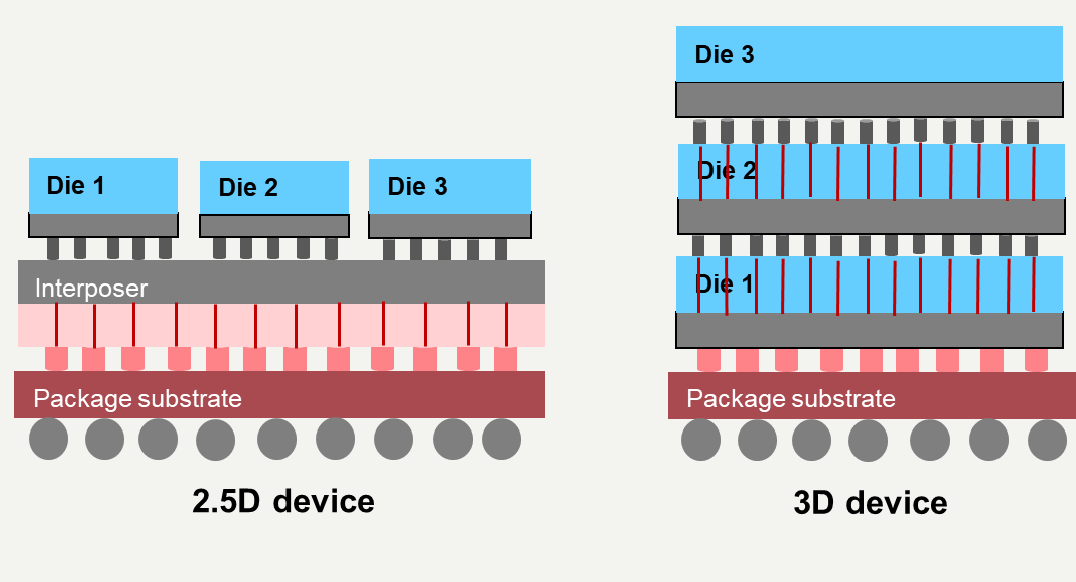
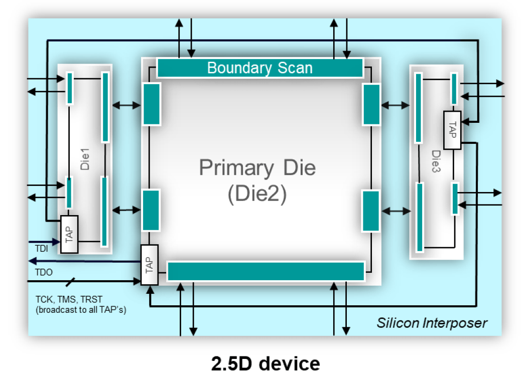
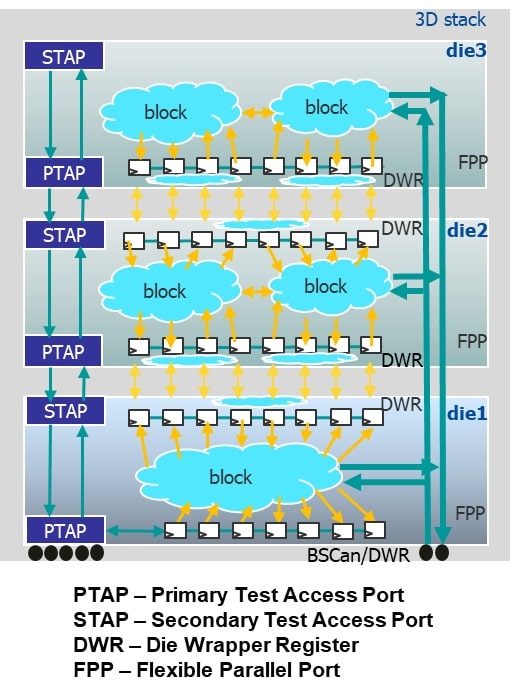
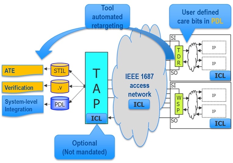
DFT Moves up to 2.5D and 3D IC


