The system design process can incorporate linear thinking, parallel thinking, or both, depending on the nature of the anticipated system, subsystem, or element of a subsystem. The structure, composition, scale, or focal point of a new/incremental system design incorporates the talents and gifts of the designer in either a top-down or bottom-up design style. Is a centralized or distributed approach to processing the best method? Is a symmetrical or asymmetrical topology warranted? Is power or speed the driving criteria? The answer to these questions can lead to a conceptual block diagram that starts the design process, leading to a design specification.
Conceptual Block Diagrams
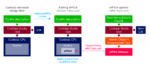
Everyone is familiar with a conceptual block diagram, where differences between block diagrams might reflect the level of abstraction, or conversely, how much detail is presented. A two-dimensional block diagram may implement a three dimensional nodal topology, or a linear communication block diagram may implement a multi-modulation scheme (Figure 1 ). After creating a conceptual block diagram, what methodologies are available to evaluate the system performance in terms of system throughput, system power, system latency, resource utilization, as related to cost? In many cases, the system throughput, power, latency, utilization, or cost are established by customers directly, or product marketing indirectly working with customers. It might be termed a marketing requirements document, a design specification, a product specification, or simply a spec sheet. There are many designations for a “design” level specification, which contains one or more conceptual block diagrams.
Design Level Specification
A design level specification captures a new or incremental approach to improving system throughput, power, latency, utilization, or cost; typically referred to as price-performance tradeoffs in product marketing. In medium to large system design organizations, a design specification may be coordinated, and, or approved by the executive staff, marketing, R&D, manufacturing, field support, or a specific customer. The degree of coordination, or approval, for system design specifications between intra-company groups varies from company to company, depending on the type of system market, time to market, consumer or industrial market segment, and market maturity. At each step in the evolution of a design specification, well-intentioned modifications, or improvements, may occur. What happens to the system design process if a well intentioned design specification change impacts the original conceptual block diagrams, such that design margin for system throughput drops from 20% to 5%? While the R&D group, who created the conceptual block diagram, may realize that the system throughput will be impacted by a marketing modification, there may not be an easy way to determine that the worst-case design margin has shrunk to 5%. Or, in other words, the time required to evaluate a design modification before, or after, the system design process has started, can vary dramatically, depending on the system evaluation methodology selected.
System Evaluation Methodologies
Moore’s law in reverse will reveal that systems created in the 1970s, or early 1980s could be designed and modified on a proverbial napkin, sent to a development team, and allow man to explore the moon on schedule, cost not withstanding. Intel’s development of the co-processor in the mid-80s marked the increasing sophistication of system design, given the transition from medium scale integration to large scale integration in chip design.
EXCEL spreadsheets became popular for estimating average throughput, power, latency, utilization, and cost at the system level when some napkin designs began to have problems in accurately estimating overall system performance, as system complexity increased. The problems encountered were mathematical discontinuities related to system operation (especially digital), estimating peak system performance, and simply mistakes in a spreadsheet, that were not readily apparent.
C and C++ golden reference models became popular in the late 1980s, and early 1990s, since they could resolve some of the EXCEL spreadsheet issues with a modest programming effort. To resolve digital system modeling issues, C/C++ provided internal synchronization in the form of software generated clocks or events, common resource objects and user-defined classes. The problems encountered were related to the envisioned “modest” programming effort. Software bugs were more difficult to find in increasingly complex software that resolved some of the EXCEL spreadsheet issues. Nonetheless, better performance modeling results were obtained with substantial programming effort. Different companies or even different groups within the same company typically made different assumptions regarding their internal golden reference models, such that it was difficult to exchange models from one company to another or one group to another group. Their golden reference models lacked a common frame of reference, or sometimes referred to as interoperability. In the early 1990s, the combination of low cost workstations, and modeling tools needing a common frame of reference started to appear in the marketplace.
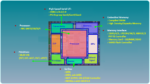
Several system level tools, such as BONeS Designer (Block-Oriented Network System Designer) (Figure 2 ), Signal Processing Workstation (SPW), OPNET Modeler, SES Workbench, CACI COMNeT and Virtual Component Co-Design (VCC) appeared to provide the notion of time-ordered, concurrent system processes, embedded software algorithms, and data types. C/C++ programming languages do not explicitly provide for time sequenced operations, parallel time sequenced operations, or design related data types. Some companies shifted from C/C++ golden reference models to these standard modeling tool methodologies. In addition, many of these tools were graphically oriented, which reduced the need for extensive C/C++ coding efforts, replacing standard modeling functionality with graphical representations of common functions. If specific functionality was required, the user could create a custom-coded element, or block, depending on the modeling libraries supported by the tool.
Graphical modeling provided additional system-level modeling capabilities:
- Ability to create hierarchical models
- Ability to handle different levels of abstraction
- Ability to speed model creation and partitioning
- Ability to spatially refine an abstract model to a more detailed model
- Ability to reuse system level modeling modules
The afore-mentioned tools focused on improving modeling capabilities in terms of performance modeling, ease of use, model creation time, and post-processing of modeling results. Some of the issues with these early system level modeling tools is that they were suited to specific classes of systems, added their own syntax to graphical modeling, and sometimes lacked sufficient libraries to solve certain modeling problems.
System Level Modeling
The system level modeling space consists of both methodology-specific and application-specific modeling domains that overlap to some extent. Methodology-specific domains consist of discrete-event, cycle-based, synchronous data flow and continuous time, models of computation provide a modeling methodology for general classes of modeling problems. The discrete-event model of computation is used for digital portions of a design that may have a strong control component. A discrete-event model of computation is very efficient for higher levels of abstraction, as the current simulation time is based on both deterministic synchronous and asynchronous events. Discrete-event models provide a user with both time-ordered (asynchronous) and concurrent (synchronous) event modeling capabilities.
A cycle-based model of computation is similar to a discrete-event model of the computation with the proviso that the model is clock-driven, executing the simulation engine for each clock cycle. Cycle-based simulators provide a user with more modeling fidelity, meaning that they usually are used for more detailed modeling of digital systems, including verification of the final design. A synchronous data flow model of computation is more DSP algorithm oriented, meaning the mathematical processing of Baseband digital signals, whether vectors, matrices, or complex data types. Internal processing of synchronous data flow type models can be simpler than a discrete-event modeling engine, requiring the concurrence of tokens at each modeling block to start processing, and the generation of new tokens to subsequent modeling blocks.
Application-specific modeling domains might include:
- Multi media (MPEG, AAC, Quick Time, etc.)
- Wireless (G3, GSM, 802.11a/b/g, Bluetooth, UWB, etc.)
- Wired (Routers, switches, etc.)
- Processors (uP, DSP, bus, cache, SDRAM, ASIC, etc.)
New Thinking
System level modeling is evolving to solve the original problem cited, how to determine quickly and efficiently how a change to a design specification might impact the performance of a proposed system. Is the throughput margin now 15% or 5%? One aspect of the system design process, the design specification itself typically remains a Word document with text, block diagrams, etc. It is difficult to exchange models with executive staff, marketing, manufacturing, or field support, simply because they lack the modeling expertise certain tools require. If the system level, or golden level model, could be exchanged among the disparate groups, or within design groups located around the globe, as part of the design specification, then the evaluation of a proposed change might be performed by the marketing organization directly.
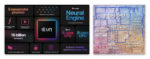
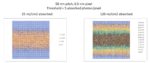
One approach is to use the power of the Web Browser and Internet-based collaboration to embed a system level model into a design specification document as a Java Applet. Companies such as Mirabilis Design of Sunnyvale California have created a methodology around this to enable design team collaboration and better communication between suppliers and system companies (Figure 3 ). Any internet browser can run a system level model embedded as a Java Applet within an HTML document. In other words, the design specification can now contain an “executable” system level model that other people within the organization can run with a net browser, no additional software or license is required. The model contained within the Java Applet is identical to the tool level model, containing all the parameters, and block attributes the original model contains. Once can modify parameters such as bus speed and input data rate, but cannot modify the base architecture and connectivity.
Similarly models must be stitched together with Intellectual Property (IP) that is produced and maintained in disparate regions of the world. The system-level models associated with these IP can be located at the source, thus ensuring the latest is always available to engineers. Using a graphical model construction environment and sophisticated search engine, the most suitable set of technology can be easily evaluated and selected based on performance/power characteristics. Updates to any technology will be immediately and automatically available at the designer’s desktop. This would be a vast improvement over current IP communication techniques that depend on expensive custom modeling effort and a transition period for the user to upgrade their database setup. Moreover the Designer has vast degrees of freedom to create a quality product.
Another part of the puzzle is a seamless integration of the disparate models of computation. Just as hardware implementation tools support mixed language mode, system tools now support a common modeling platform. For example, Synopsys integrated Cossap (dynamic data flow) and SystemC (digital) into System Studio while VisualSim from Mirabilis Design combines SystemC (digital), synchronous dataflow (DSP), finite state machine (FSM), and continuous time (analog) domains. Previous system level tools typically supported a single modeling specific domain. Additionally, making the modeling software platform to be Operating System agnostic reduces support cost and enables easy data transition across the company.
Finally, a new approach to standard library development is required. Prior generations of graphical modeling tools might advertise 3,000 plus libraries as a sign of modeling tool maturity and robustness. However, if a new Ultra-Wideband model was required, then most of the prior libraries may not be reusable for UWB, since many were prior generation application specific type libraries, or bottom-up component libraries. A new system level modeling approach will not measure the tool by the quantity of libraries, rather by the quality and integration of the system level libraries. Such libraries will have a high likelihood of reuse in a new technology, or system level model. Relative to prior generations of graphical modeling tools, VisualSim integrates as many as thirty bottom-up component functions into a single, system level, easy to use, reusable block, or module. Four VisualSim queue blocks replace 24 prior generation queue blocks through polymorphic port support, block level menu attributes, while improving simulation performance.
For more information: https://www.mirabilisdesign.com/contact/
About the Authors:
Darryl Koivisto is the CTO at Mirabilis Design. Dr. Koivisto has a Ph.D. from Golden Gate University, MS from Santa Clara University and BS from California Polytechnic University, San Luis Obispo.
Deepak Shankar is Founder at Mirabilis Design. Mr. Shankar has an MBA from UC Berkeley, MS from Clemson University and BS from Coimbatore Institute of Technology.
Also read:
System-Level Modeling using your Web Browser