Neural network models are advancing rapidly and becoming more complex. Application developers using these new models need faster AI inference but typically can’t afford more power, space, or cooling. Researchers have put forth various strategies in efforts to wring out more performance from AI inference architectures, most notably placing parallelized execution and memory resources closer together. Compute-in-memory takes memory locality to the extreme by combining memory accesses and execution in a single operation – however, it comes with the risks and complexity of analog design and fabrication. Expedera’s new white paper examines compute-in-memory in AI inference and explores the tradeoffs versus its all-digital compute-near-memory solution optimizing all neural network processing elements.
Motivation for compute-in-memory technology
What’s the most expensive operation for a CPU? Moving data. It keeps operations from running and forms nasty bottlenecks if too much flows simultaneously. Manycore solutions like GPUs help multiplier performance but don’t eliminate the data movement penalties. Neither CPUs nor GPUs are efficient for AI inference, opening a door for the NPU (neural processing unit), seeking balance for efficient parallel execution with effective data access.
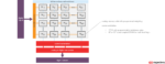
Instead of placing execution cores over here, a pile of memory over there, and a bus in between, one path to faster data access is locality – for which three basic strategies exist:
- Compute-near-memory spreads smaller blocks of memory nearby blocks of execution units but not necessarily partitioned in a one-to-one relationship.
- Compute-at-memory tightly couples an execution unit with its supporting memory, forming a co-processor unit that can be stepped and replicated for scale.
- Compute-in-memory changes the memory structure by physically embedding a multiplier unit in a customized unit, so a memory read fetches a pre-multiplied result.
Saying compute-in-memory “changes the structure” may be understated. Both compute-near-memory and compute-at-memory use a conventional digital multiplier. Compute-in-memory relies on an incoming digital word triggering analog technology for multiplication and current summing. An analog-to-digital converter is required to get the result back to digital.
Conceptually, the neural network weight coefficients stay put in a compute-in-memory scheme and are always at hand for rapid multiplication with the data of interest. Cutting out data movements and streamlining operations trims AI inference time, and fewer transistors in action can mean lower power consumption. Those are good outcomes, right?
Throughput is only one factor for compute-in-memory in AI inference
Unsurprisingly, some tradeoffs arise. Some issues are inherent to the compute-in-memory structure, and some relate to the overall design and fabrication cycle.
A significant advantage of digital circuitry is noise immunity. Moving operations back into analog reintroduces noise factors and analog variation that limit realizable bit precision; researchers seem confident in 4-bit implementations. Lower AI inference precision raises demands on AI training, with more cycles required for reliable inference. Achieving higher precision, say int8, also introduces problems. The analog transistor array becomes much more complex, as does the analog-to-digital converter needed. Area and power consumption savings are offset, and the chance for bit errors rises as analog step width shrinks.
It’s certainly possible to size, interconnect, and optimize a compute-in-memory array for a particular inference model or group of similar complexity models. But, as we’ve discussed elsewhere, that removes flexibility, and the risk grows if a different model is needed. Other hits on flexibility are locking into specific, transistor-level modifications in a selected memory technology, and placement and routing constraints may appear at the system-on-chip level.
Moving into analog also means moving into a mixed-signal foundry process. Advanced nodes may be entirely off the table for some time. It also means analog expertise and tools are required, and it is difficult to scale layouts with analog circuitry.
Achieving better performance gains in all-digital NPU IP
Substantial engineering effort is often necessary to wring the last percentage points of performance out of an application unless conditions align perfectly where a bit more is possible. Use cases for compute-in-memory in AI inference will probably look like this:
- Models with large numbers of weight coefficients, fully connected layers, and sparse activations
- Int4 precisions where extended AI training is feasible and analog noise immunity is better
- Scale compatible with mature mixed-signal process technology and wafer costs
Still, we’re not talking about something like a 4x performance gain with compute-in-memory compared to all-digital NPU IP. Remember that compute-in-memory is only one small part of a complete NPU solution, and performance improvements are available at other points around the core multiply operation. But are they worth the risks and costs of the analog environment?
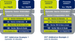
Expedera’s value proposition is straightforward. Using high-efficiency all-digital NPU IP, combining scalable hardware with packet-based sequencing directed by compiler software, Expedera teams working with OEMs deliver better performance gains in a complete AI inference solution. As Expedera’s IP evolves and process technology advances, it gets faster, smaller, and more power efficient, and it can be customized for OEM requirements.
Compute-in-memory and Expedera NPU IP are independent of each other – both will exist in the market once compute-in-memory gains more adoption. There’s more to read about both approaches in the full Expedera white paper; simple registration gets a download.
Architectural Considerations for Compute-in-Memory in AI Inference
Also Read:
Deep thinking on compute-in-memory in AI inference
Area-optimized AI inference for cost-sensitive applications