

Artificial intelligence (AI) is transforming many aspects of our lives, from the way we work and communicate to the way we shop and travel. Its impact is felt in nearly every industry, including the semiconductor industry, which plays a crucial role in enabling the development of AI technology.
One of the ways AI is affecting our daily lives is by making everyday tasks more efficient and convenient. For example, AI-powered virtual assistants such as Alexa and Siri can help us schedule appointments, set reminders, and answer our questions. AI algorithms are also being used in healthcare to analyze patient data and provide personalized treatment plans, as well as in finance to detect fraud and make investment decisions.
AI is also changing the way we work. Many jobs that used to require human labor are now being automated using AI technology. For example, warehouses are increasingly using robots to move and sort goods, and customer service departments are using chatbots to handle routine inquiries.
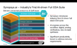
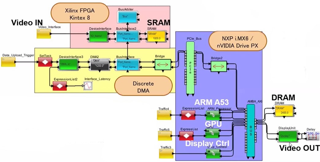
The semiconductor industry is a critical component of the AI revolution. AI relies on powerful computing processors, such as graphics processing units (GPUs) and deep learning processors (DLPs), to process massive amounts of data and perform complex calculations. The demand for these chips has skyrocketed in recent years, as more companies invest in AI technology.
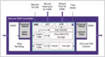
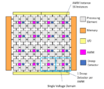
AI is beginning to have an impact on the design and verification of ICs. AI can be used to improve the overall design process by providing designers with new tools and insights. For example, AI-powered design tools can help designers explore design alternatives and identify tradeoffs between performance, power consumption, and cost. AI can also be used to provide designers with insights into the behavior of complex systems, such as the interaction between software and hardware in an embedded system.
AI is enabling the development of new types of chips and systems. For example, AI is driving the development of specialized chips for specific AI applications, such as image recognition and natural language processing. These specialized chips can perform these tasks much faster and more efficiently than general-purpose processors and are driving new advances in AI technology.
Semiconductor fabrication is the largest expenditure and AI has the greatest potential in this area. AI can help optimize the manufacturing process from design to fabrication by analyzing the process data, identifying defects, and suggesting optimizations. These insights and changes will allow fans to detect problems earlier, reducing cost, increasing yield, and improving overall efficiency.
There are also many concerns with a technology that is this disruptive. While this automation can potentially increase productivity and reduce costs, it also raises concerns about job loss and the need for workers to acquire new skills. There are also a number of ethical concerns associated with AI. AI systems can collect and analyze large amounts of personal data, raising concerns about privacy and surveillance. There are also concerns about the potential for corporations and governments to misuse this data for their own purposes.
AI is transforming many aspects of our lives, from the way we work and communicate to the way we shop and travel. The semiconductor industry is a critical component of the AI revolution, not only providing the computing power to enable AI, but also benefiting from AI for IC design and manufacturing improvements. As AI technology continues to advance, it is likely that it will continue to play an increasingly important role in the semiconductor design process, enabling new levels of innovation and driving new advances in AI technology. It is essential to stay informed about AIs impact and ensure that its benefits are realized while minimizing the potential risks.
Also Read:
Narrow AI vs. General AI vs. Super AI
Scaling AI as a Service Demands New Server Hardware


