Generative AI has been making waves across various industries, and its potential continues to expand. Among its many applications, one particularly intriguing area is the capacity of GenAI to explain digital design waveforms and act as a co-pilot for hardware engineers in the debugging process. In this article, we will explore the fascinating possibilities that this technology brings to the table and its impact on the field of silicon development.
Experiment 2: Explaining Design Waveforms
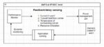
This first experiment showcases the ability of Generative AI to recognise patterns and trends in data and revolutionise the way we understand and interact with waveforms. In this experiment, Google’s Generative AI Model – BARD was used to generate an explanation of write transfers in a system complying to AMBA APB protocol by looking at a sample waveform (sourced from https://documentation-service.arm.com)
Generated Explanation (tweaked to make its language inclusive)
Disclaimer: This explanation is not reviewed for accuracy

The waveform in the image shows the following signals:

TCLK: The APB3 clock signal.
PADDR: The APB3 address bus.
PWRITE: The APB3 write signal.
PSEL: The APB3 chip select signal.
PENABLE: The APB3 enable signal.
PWDATA: The APB3 write data bus.
PREADY: The APB3 ready signal.
Data 1: The data being written to the APB3 completer device.

The waveform shows the following behavior:

At time T1, the PWRITE signal goes high and the PADDR bus is driven with the address of the APB3 completer device to be written to.

At time T2, the PSEL signal goes high. This indicates that the APB3 initiator is ready to transfer data to the completer device.

At time T3, the PENABLE signal goes high. This indicates that the APB3 initiator is ready to drive the PWDATA bus.

At time T4, the PREADY signal goes high. This indicates that the APB3 completer device is ready to receive the data on the PWDATA bus.

At time T5, the PWRITE signal goes low. This indicates that the APB3 initiator has finished transferring data to the completer device.

The PSEL and PENABLE signals remain high until the APB3 completer device has finished processing the data.
What Does Future Look Like – GenAI Powered Debugger Copilot
One of the most exciting applications of generative AI is the potential it holds to be a co-pilot for developers during the debugging process. Waveforms are the lifeblood of complex systems in hardware design. A debugger copilot, powered by generative AI, can dissect waveforms, identify anomalies, and correlate patterns, making it an invaluable tool for engineers seeking to comprehend complex design behavior.
Challenges in Developing a Debugger Copilot
While the prospects of a debugger copilot powered by generative AI are enticing, there are challenges that need to be addressed. The accuracy and reliability of the AI’s explanations are paramount. We must ensure that the AI’s insights are trustworthy and not just algorithmically generated responses. Moreover, privacy and data security concerns are significant. Handling sensitive information in the debugging process requires a robust framework to protect data integrity.
Conclusion
The journey of generative AI into the realm of explaining waveforms and acting as a debugger copilot is an exciting one. This technology has the potential to transform the way we develop and debug software, saving time, reducing costs, and increasing accuracy. As engineers continue to explore its possibilities, the future of debugging looks promising.