Today’s power modeling solutions are trained at measuring power using the micro-events captured from detailed RTL simulation or studying the electromagnetic radiation from IR drop and side channel attacks. These solutions are fantastic for debugging and verification of the implementation. There are both open source and commercial products for power modeling. For example, Synopsys PrimeTime can provide the percentage of activity in a stage for each device while Cadence Joules can debug the power intent, and Ansys Totem can help with the transistor-level power integrity and reliability analysis. There is an open-source power modelling add-on to SystemC. All of these are static solutions that take the simulation, process it and generate reports. Alternately they work in conjunction with a debugger.
As the power requirements get more stringent and complex, designers need to predict the power consumption, impact of power intent and savings from power management units, during architecture exploration. System designers and integrators want the power consumption metrics in the datasheet for the entire activity range, not just one or two scenarios. The marketing team must be able to quickly generate power metrics for the requested scenarios. Thermal team requires heat and temperature data to plan for the cooling, chassis design and board layout. The system integrators need guidelines on the battery lifecycle and peak power to plan for the supply and capacitance. Thus, a good modelling solution must support power generation, storage, analog and digital consumption and power management. The IP or semiconductor vendor must have the ability share a dynamic model that quickly simulate scenarios. The accuracy of the power measurements at the architecture exploration must be within 10% of the value at RTL or board-level.
Power exploration starts by examining the tangible hardware and software choices that significantly affect SoC power consumption. These include:
- Use cases
- Architectural details (number of cores, choice of accelerators)
- Power-saving features (DVFS, clock gating, power gating)
- Firmware/software algorithms
- Operating frequency and voltage modes
- Process technology aspects that impact power
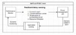
Modern SOCs employ multiple power management strategies either at individual IP level or full SOC level. One such strategy is adaptive voltage and frequency scaling (AVFS). In AVFS, a closed-loop feedback system is implemented between the voltage scaling power supply and delay-sensing performance monitor on the SoC. The on-chip performance monitor not only sees the actual voltage delivered on-chip but also understands whether the silicon is slow, typical or fast, and the effect of the temperature of the surrounding silicon. It can also track the utilization parameters to decide the choice of operating points.
The figure below represents an example of this feedback system between power manager and performance monitor on a chip.
System-level modelling solutions such as VisualSim Power Modeler 2.0 can be used to model the effect of power management strategies on the system performance and hence decide on a power-performance trade-off in early system design phases.
In the intricate realm of System-on-Chip (SoC) design, optimizing power is paramount. VisualSim Power Modeling 2.0 is a dynamic power exploration, optimization and measurement of the Intellectual Property, Semiconductor Device, embedded system, chassis or Data Center. VisualSim enables system-level SoC power measurement even before delving into the intricacies of Register Transfer Level (RTL) development. Using this solution, designers and Power Architect can study ways to reduce power consumption, measure power consumed for a software application, impact of hardware configurations, adding of new hardware or change in the interconnect and new workloads/ use-cases. As the Power modeling toolkit is common from IP vendors to the system deployment, it is possible for suppliers and the system integrators to share encrypted power information along with the model.
VisualSim System-Level Power Modeling is used during the specification phase and before development. Thus, it is possible to optimize the architecture to achieve Power-Performance-Trade off before development and also reuse the model for downstream debugging.
The built-AI engine continuously monitors the power activity to identify failures and identifies the cause of the failure.
See Webinar Replays Here
Also Read:
System Simulation, Architecture Exploration, Power Management, Performance Analysis
Mirabilis Invites System Architects at DAC 2023 in San Francisco