

Chiplets (die stacking) is not new. The origins are deeply rooted in the semiconductor industry and represent a modular approach to designing and manufacturing integrated circuits. The concept of chiplets has been energized as a response to the recent challenges posed by the increasing complexity of semiconductor design. Here are some well documented points about the demand for chiplets:
Complexity of Integrated Circuits (ICs): As semiconductor technology advanced, the complexity of designing and manufacturing large monolithic ICs increased. This led to challenges in terms of yield, cost, skilled resources, and time-to-market.
Moore’s Law: The semiconductor industry has been following Moore’s Law, which suggests that the number of transistors on a microchip doubles approximately every two years. This relentless scaling of transistor density poses challenges for traditional monolithic designs.
Diverse Applications: Different applications require specialized components and features. Instead of creating a monolithic chip that tries to cater to all needs, chiplets allow for the creation of specialized components that can be combined in a mix-and-match fashion.
Cost and Time-to-Market Considerations: Developing a new semiconductor process technology is an expensive and time-consuming endeavor. Chiplets provide a way to leverage existing mature processes for certain components while focusing on innovation for specific functionalities. Chiplets also aid in the ramping of new process technologies since the die sizes and complexity are a fraction of a monolithic chip thus easing manufacturing and yield.
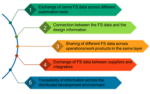
Interconnect Challenges: Traditional monolithic designs faced challenges in terms of interconnectivity as the distance between components increased. Chiplets allow for improved modularity and ease of interconnectivity.
Heterogeneous Integration: Chiplets enable the integration of different technologies, materials, and functionalities on a single package. This approach, known as heterogeneous integration, facilitates the combination of diverse components to achieve better overall performance.
Industry Collaboration: The development of chiplets often involves collaboration between different semiconductor companies and industry players. Standardization efforts, such as those led by organizations like the Universal Chiplet Interconnect Express Consortium (UCIe) for chiplet integration.
Bottom line: Chiplets emerged as a solution to address the challenges posed by the increasing complexity, cost, time-to-market, and staffing pressures in the semiconductor industry. The modular and flexible nature of chiplet-based designs allows for more efficient and customizable integration of chips, contributing to advancements in semiconductor technology, not to mention the ability to multi source die.
Intel
Intel really has capitalized on chiplets which is key to their IDM 2.0 strategy.
There are two major points:
Intel will use chiplets to deliver 5 process nodes in 4 years which is a critical milestone in the IEDM 2.0 strategy (Intel 7, 4, 3, 20A, 18A).
Intel developed the Intel 4 process for internal products using chiplets. Intel developed CPU chiplets which is much easier to do than the historically monolithic CPU chips. Chiplets can be used to ramp a process much quicker and Intel can claim success without having to do a full process for complex CPUs or GPUs. Intel can then release a new process node (Intel 3) for foundry customers which can design monolithic or chiplet based chips. Intel is also doing this for 20A and 18A thus the 5 process nodes in 4 years milestone. This accomplishment is debatable of course but I see no reason to.
Intel will use chiplets in order to outsource manufacturing (TSMC) when business dictates.
Intel signed a historical outsourcing agreement with TSMC for chiplets. This is a clear proof of concept to get us back to the multi sourcing foundry business model that we enjoyed up until the FinFET era. I do not know if Intel will continue to use TSMC beyond the N3 node but the point has been made. We are no longer bound by a single source for chip manufacturing.
Intel can use this proof of concept (using chiplets from multiple foundries and packaging them up) for foundry business opportunities where customers want the freedom of multiple foundries. Intel is the first company to do this.
TSMC
There are two major points:
Using chiplets customers can theoretically multi source where their die comes from. Last I heard TSMC would not package die from other foundries but if a whale like Nvidia asked them to I’m sure they would.
Chiplets will challenge TSMC and TSMC is always up for a challenge because with challenge comes innovation.
TSMC quickly responded to chiplets with their 3D Fabric comprehensive family of 3D Silicon Stacking and Advanced Packaging Technologies. The greatest challenge for chiplets today is the supporting ecosystem and that is what TSMC is all about, ecosystem.
Back to the original question “How Disruptive will Chiplets be for Intel and TSMC?” Very much so. We are in the beginning of a semiconductor manufacturing disruption that we have not seen since FinFETs. All pure-play and IDM foundries now have the opportunity to get a piece of the chips that the world depends on, absolutely.
Also Read:
2024 Big Race is TSMC N2 and Intel 18A
IEDM: What Comes After Silicon?
IEDM: TSMC Ongoing Research on a CFET Process
IEDM Buzz – Intel Previews New Vertical Transistor Scaling Innovation


