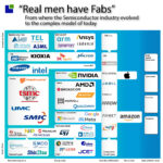
SiC Forum2025 8 Static v3

Fast Path to Baby Llama BringUp at the Edge

Fast Path to Baby Llama BringUp at the Edge
by Bernard Murphy on 09-26-2023 at 10:00 am

Baby Llama min

Tis the season for transformer-centric articles apparently – this is my third within a month. Clearly this is a domain with both great opportunities and challenges: extending large language model (LLM) potential to new edge products and revenue opportunities, with unbounded applications and volumes yet challenges in meeting performance, power, and cost goals. Which no doubt explains the explosion in solutions we are seeing. One dimension of differentiation in this race is in the underlying foundation model, especially GPT (OpenAI) versus Llama (Meta). This does not reduce to a simple “which is better?” choice it appears, rather opportunities to show strengths in different domains.

Llama versus other LLMs

GPT has enjoyed most of the press coverage so far but Llama is demonstrating it can do better in some areas. First a caveat – as in everything AI, the picture continues to change and fragment rapidly. GPT already comes in 3.5, 4, and 4.5 versions, Google has added Retro, LaMDA and PaLM2, Meta has multiple variants of Llama, etc, etc.

GPT openly aims to be king of the LLM hill both in capability and size, able from a simple prompt to return a complete essay, write software, or create images. Llama offers a more compact (and more accessible) model which should immediately attract edge developers, especially now that the Baby Llama proof of concept has been demonstrated.

GPT 4 is estimated to run to over a trillion parameters, GPT 3.5 around 150 billion, and Llama 2 has variants from 7 to 70 billion. Baby Llama is now available (as a prototype) in variants including 15 million, 42 million and 110 million parameters, a huge reduction making this direction potentially very interesting for edge devices. Notable here is that Baby Llama was developed by Andrej Karpathy of OpenAI (not Meta) as a weekend project to prove the network could be slimmed down to run on a single core laptop.

As a proof of concept, Baby Llama is yet to be independently characterized or benchmarked, however Karpathy has demonstrated ~100 tokens/second rates when running on an M1 MacBook Air. Tokens/second is a key metric for LLMs in measuring throughput in response to a prompt.

Quadric brings Baby Llama up on Chimera core in 6 weeks

Assuming that Baby Llama is a good proxy for an edge based LLM, Quadric made the following interesting points. First, they were able to port the 15 million parameter network to their Chimera core in just 6 weeks. Second, this port required no hardware changes, only some (ONNX) operation tweaking in C code to optimize for accuracy and performance. Third they were able to reach 225 tokens/second/watt, using a 4MB L2 memory, 16 GB/second DDR, a 5nm process and 1GHz clock. And fourth the whole process consumed 13 engineer weeks.


By way of comparison, they ran the identical model on an M1-based Pro laptop running the ONNX runtime with 48MB RAM (L2 + system cache) and 200 GB/sec DDR, with a 3.3 GHz clock. That delivered 11 tokens/second/watt. Quadric aims to extend their comparison to edge devices once they arrive.

Takeaways

There are obvious caveats. Baby Llama is a proof of concept with undefined use-rights as far as I know. I don’t know what (if anything) is compromised in reducing full Llama 2 to Baby Llama, though I’m guessing for the right edge applications this might not be an issue. Also performance numbers are simulation-based estimates, comparing with laptop performance rather than between implemented edge devices.

What you can do with a small LLM at the edge has already been demonstrated by recent Apple IoS/MacOS releases which now support word/phrase completion as you type. Unsurprising – next word/phrase prediction is what LLMs do. A detailed review from Jack Cook suggests their model might be a greatly reduced GPT 2 at about 34 million parameters. Unrelated recent work also suggests value for small LLMs in sensing (e.g. for predictive maintenance).

Quadric’s 6-week port with no need for hardware changes is a remarkable result, important as much in showing the ability of the Chimera core to adapt easily to new networks as in the performance claims for this specific example. Impressive! You can learn more about this demonstration HERE.

Also Read:

Vision Transformers Challenge Accelerator Architectures

An SDK for an Advanced AI Engine

Quadric’s Chimera GPNPU IP Blends NPU and DSP to Create a New Category of Hybrid SoC Processor


Optimizing Shift-Left Physical Verification Flows with Calibre

Optimizing Shift-Left Physical Verification Flows with Calibre
by Peter Bennet on 09-26-2023 at 6:00 am

Shift-left with Calibre

Advanced process nodes create challenges for EDA both in handling ever larger designs and increasing design process complexity.

Shift-left design methodologies for design cycle time compression are one response to this. And this has also forced some rethinking about how to build and optimize design tools and flows.

SemiWiki covered Calibre’s use of a shift-left strategy to target designer productivity a few months ago, focusing on the benefits this can deliver (the “what”). This time we’ll look closer at the “how” – specifically what Siemens call Calibre’s four pillars of optimization (these diagrams are from the Siemens EDA paper on this theme).

Optimizing Physical Verification (PV) means both delivering proven signoff capabilities in a focused and efficient way in the early design stages and extending the range of PV.

Efficient tool and flow Execution isn’t only about leading performance and memory usage. It’s also critical to reduce the time and effort to configure and optimize run configurations.

Debug in early stage verification is increasingly about being able to isolate which violations need fixing now and providing greater help to designers in quickly finding root causes.

Integrating Calibre Correction into the early stage PV flow can save design time and effort by avoiding potential differences between implementation and signoff tool checks.

Reading through the paper, I found it helpful here to think about the design process like this:

Current design

  • The portion of the design (block, functional unit, chip) we’re currently interested in
  • Has a design state, e.g. pre-implementation, early physical, near final, signoff

Design context

  • States of the other design parts around our current design

Verification intent

  • What we need to verify now for our current design
  • A function of current design state, context and current design objectives and priorities
  • Frequently a smaller subset of complete checks

We’ll often have a scenario like that below.

Sometimes we’ll want to suppress checks or filter out results from earlier stage blocks. Sometimes we might just want to check the top-level interfaces. Different teams may be running different checks on the same DB at the same time.

Verification configuration and analysis can have a high engineering cost. How to prevent this multiplying up over the wide set of scenarios to be covered as the design matures ? That’s the real challenge Calibre sets out to meet here by communicating a precise verification intent for each scenario, minimizing preparation, analysis, debug and correction time and effort.

Extending Physical Verification

Advanced node physical verification has driven some fundamental changes in both how checks are made and their increased scope and sophistication in the Calibre nmPlatform

Equation-based checks (eqDRC) that require complex mathematical equations using the SVRF (standard verification rule) format are one good example. And also one that emphasizes the importance of more programmable checks and fully integrating both checks and results annotation into the Calibre toolsuite and language infrastructure.

PERC (programmable electrical rule checking) is another expanding space in verification that spans traditional ESD and latch-up to newer checks like voltage dependent DRC.

Then there are thermal and stress analysis for individual chips and 3D stacked packages and emerging techniques like curvilinear layout checks for future support.

The paper provides a useful summary diagram (in far more detail than we can cover here).


Improving Execution Efficiency

EDA tool configuration is a mix of top-down (design constraints) and bottom-up (tool and implementation settings) – becoming increasingly bottom-up and complex as the flow progresses. But we don’t want all the full time-consuming PV config effort for the early design checks in a shift-left flow.

Calibre swaps out the traditional trial-and-error config search for a smarter, guided and AI-enabled one which understands the designer’s verification intent. Designers might provide details on the expected state (“cleanliness”) of the design and even relevant error types and critical parts of a design, creating targeted check sets that minimize run time.

Some techniques used by Calibre are captured below.


Accelerating Debug

Streamlining checks for the design context usefully raises the signal-to-noise ratio in verification reports. But there’s still work to do in isolating which violations need addressing now (for example, a designer may only need to verify block interfaces) and then finding their root causes.

Calibre puts accumulated experience and design awareness to work to extract valuable hints and clues to common root causes – Calibre’s debug signals. AI-empowered techniques aid designers in analyzing, partitioning, clustering and visualizing the reported errors.

Some of Calibre’s debug capabilities are shown below.


Streamlining Correction

If we’re running Calibre PV in earlier design stages, why not use Calibre’s proven correct-by-construction layout modifications and optimizations from its signoff toolkit for the fixes – eliminating risks from potential differences in implementation and signoff tool checks ? While Calibre’s primarily a verification tool, it’s always had some design fixing capabilities and is already tightly integrated with all leading layout flows.

But the critical reason is that layout tools aren’t always that good at some of the tasks they’ve traditionally been asked to do. Whether that’s slowness in the case of filler insertion or lack of precision in what they do – since they don’t have signoff quality rule-checking – meaning either later rework or increased design margining.

An earlier SemiWiki article specifically covered Calibre Design Enhancer’s capabilities for design correction.

The paper shows some examples of Calibre optimization.


Summary

A recent article about SoC design margins noted how they were originally applied independently at each major design stage. As diminishing returns from process shrinks exposed the costly over-design this allowed, this forced a change to a whole process approach to margining.

It feels like we’re at a similar point with the design flow tools. No longer sufficient to build flows “tools-up” and hope that produces good design flows, instead move to a more “flow-down” approach where we co-optimize EDA tools and design flows.

That’s certainly the direction Calibre’s shift-left strategy is following. building on these four pillars of optimization.

Find more details in the original Siemens EDA paper here:

The four foundational pillars of Calibre shift-left solutions for IC design & implementation flows.


Power Analysis from Software to Architecture to Signoff

Power Analysis from Software to Architecture to Signoff
by Daniel Payne on 09-25-2023 at 10:00 am

power analysis min

SoC designs use many levels of design abstraction during their journey from ideation to implementation, and now it’s possible to perform power analysis quite early in the design process. I had a call with William Ruby, Director of Porduct Marketing – Synopsys Low Power Solution to hear what they’ve engineered across multiple technologies.  Low-power IC designs that run on batteries need to meet battery life goals, and that is achieved through analyzing and minimizing power throughout the design lifecycle. High-performance IC designs also need to meet their power specifications, and lowering power during early analysis can also allow for increased clock rates which then boosts performance further. There are five EDA products from Synopsys that each provide power analysis and optimization capabilities to your engineering team from software to signoff.

Power-aware tools at Synopsys

The first EDA tool listed is Platform Architect, and that is used to explore architectures and even provide early power analysis, before any RTL is developed by using an architectural model that your team can run different use cases on. With the Platform Architect tool you can build a virtual platform for early software development, and to start verifying the hardware performance.

Once RTL has been developed, then an emulator like Synopsys ZeBu can be used to run actual software on the hardware representation. Following the emulation run, ZeBu Empower delivers power profiling of the entire SoC design so that you can know the sources of dynamic and leakage power quite early, before silicon implementation. These power profiles cover billions of cycles, and the critical regions are quickly identified as areas for improvements.

Zebu Empower flow

RTL Power Analysis

RTL power analysis is run with the PrimePower RTL tool using vectors from simulation and/or emulation, or even without vectors for what-if analysis. Designers can explore and get guidance on the effects of clock-gating, memory, data-path and glitch power. The power analysis done at this stage is physically-aware, and consistent with signoff power analysis results.

PrimePower – Three Stages

Gate-level Power Analysis

Logic synthesis converts RTL into a technology-specific gate-level netlist, ready for placement and routing during the implementation stage. The golden power signoff is done on the gate-level design using PrimePower. Gate-level power analysis provides you with average power, peak power, glitch power, clock network power, dynamic and leakage power, and even multi-voltage power. Input vectors can come from RTL simulation, emulation or vectorless. The RTL to GDSII flow is provided with the Fusion Compiler tool, where engineers optimize their Power, Performance and Area (PPA) goals.

Summary

Achieving energy efficiency from software to silicon is now a reality using the flow of tools and technologies provided by Synopsys. This approach takes the guesswork out of meeting your power goals prior to testing silicon, and has been proven by many design teams around the world. What a relief to actually know that your power specification has been met early in the design lifecycle.

Synopsys has a web page devoted to energy-efficient SoC designs, and there’s even a short overview video on low-power methodology. There’s also a White Paper, Achieving Consistent RTL Power Accuracy.

Related Blogs


WEBINAR: Why Rigorous Testing is So Important for PCI Express 6.0

WEBINAR: Why Rigorous Testing is So Important for PCI Express 6.0
by Daniel Nenni on 09-25-2023 at 8:00 am

PCIe IO bandwidth doubles every 3 years

In the age of rapid technological innovation, hyperscale datacenters are evolving at a breakneck pace. With the continued advancements in CPUs, GPUs, accelerators, and switches, faster data transfers are now paramount. At the forefront of this advancement is PCI Express (PCIe®), which has become the de-facto standard of interconnect for high-speed data transfers between processing and computing nodes.

Click here to register now!

Doubling Data Rates: The Trend Continues

The PCI-SIG® consortium, responsible for the PCIe interface, has a history of launching a new PCIe generation approximately every three years. This invariably has doubled the data rate over the past decade. PCI-SIG’s latest release, PCIe 6.0.1, ushers in multi-level Pulse Amplitude Modulation (PAM4) signaling, boasting a staggering transfer rate of 64 GT/s in one direction on a single lane. Notably, during the 2022 PCI-SIG DevCon, the announcement of PCIe 7.0 specification came, doubling the data rate to 128 GT/s, emphasizing both power efficiency and higher bandwidth.

Figure 1. PCI-SIG I/O Bandwidth doubles every 3 years. From PCI-SIG

 Stringent Testing for Compliance and Interoperability

It’s important to understand that beyond hyperscale data centers, the deployment of PCIe technology in fields like handheld devices, servers, automotive, industrial applications, and more demands high reliability and cost-effectiveness. This necessitates rigorous compliance testing for products to ensure they align with the PCIe 6.0.1 specification and can successfully interoperate with other PCIe devices.

Unveiling PAM4 Signaling and its Implications

The integration of PAM4 signaling in PCIe 6.0.1 is key. Unlike the Non-Return-to-Zero (NRZ) signaling, which used two distinct signal levels, PAM4 uses four, transmitting two bits of information within a single unit interval (UI). This modification introduces new challenges like cross-talk interferences, signal reflections, and power supply noise. The PCIe 6.0.1 specification has introduced the Signal-to-Noise Distortion Ratio (SNDR) to address these challenges, encapsulating both the traditional noise and non-compensable impairments within the electrical signal. Understanding of signal integrity issues in the high-speed communication channels due to cross-talk, reflection losses with frequency and time domain analysis  is the key. Channel measurement techniques and various signal enhancement techniques with PCIe 6.0 Transmitter and Receiver equalization are used to compensate for non-ideal channel characteristics.

Summary

The advancements in PCIe technology have paved the way for a new age of data transfer capabilities, with PCIe 6.0.1 and the forthcoming PCIe 7.0 setting new benchmarks. However, with greater capabilities come greater challenges, particularly in ensuring compliance and interoperability. Partnerships like Synopsys and Tektronix are leading the charge in addressing these challenges, ensuring that the technology not only meets but exceeds the demands of today’s digital age.

Join Our Webinar!

Want to delve deeper into PCIe simulations and electrical testing? Join our upcoming webinar on Tuesday October 10, from 9:00 am to 10:00 am PDT, where Synopsys and Tektronix industry experts will discuss the latest in PCIe technology and the significance of robust testing methodologies. Click here to register now!

Speakers:

David Bouse is a Principal Technology Leader at Tektronix and an active contributor to PCI-SIG with expertise in highspeed SERDES including transmitter and receiver test methodologies, DSP algorithms for NRZ/PAM4 signaling, clock characterization, and automation software architecture.

Madhumita Sanyal is a Sr. Staff Technical Manager for Synopsys high-speed SerDes portfolio. She has +17 years of experience in design and application of ASIC WLAN products, logic libraries, embedded memories, and mixed-signal IP.

About Synopsys

Synopsys, Inc. (Nasdaq: SNPS) is the Silicon to Software™ partner for innovative companies developing the electronic products and software applications we rely on every day. As an S&P 500 company, Synopsys has a long history of being a global leader in electronic design automation (EDA) and semiconductor IP and offers the industry’s broadest portfolio of application security testing tools and services. Whether you’re a system-on-chip (SoC) designer creating advanced semiconductors, or a software developer writing more secure, high-quality code, Synopsys has the solutions needed to deliver innovative products. Learn more at www.synopsys.com.

Also Read:

Next-Gen AI Engine for Intelligent Vision Applications

VC Formal Enabled QED Proofs on a RISC-V Core

Computational Imaging Craves System-Level Design and Simulation Tools to Leverage AI in Embedded Vision


TSMC’s First US Fab

TSMC’s First US Fab
by Daniel Nenni on 09-25-2023 at 6:00 am

WaferTech TSMC

TSMC originally brought the pure-play foundry business to the United States in 1996 through a joint venture with customers Altera, Analog Devices, ISSI, and private investors (no government money). Altera is now part of Intel but ADI is still a top TSMC customer and enthusiastic supporter. I have seen the ADI CEO Vincent Roche present at recent TSMC events and his TSMC partnership story is compelling. This joint venture was part of TSMC’s customer centric approach to business, responding directly to customer requests.

The WaferTech fab was established in Camas Washington (just North of the Oregon/Washington border) in 1996 with an investment of more than $1B which was a huge amount of money at the time. Production started two years later at .35 micron which was part of the Philips technology transfer that TSMC was founded upon. In 2000 TSMC bought out the partners and private investors, taking full control of the Washington fab. It is now called TSMC Fab 11 but clearly this fab was ahead of its time, absolutely.

From TSMC:

WaferTech focuses on Embedded Flash process technology while supporting a broad TSMC technology portfolio on line-widths ranging from 0.35-microns down to 0.16-microns. We specialize in helping companies deliver differentiated products and work with them on a number of customized and manufacturing “phase-in” projects. As a result, WaferTech delivers the latest generation semiconductors around the globe, supporting innovations in automotive, communications, computing, consumer, industrial, medical and military/aerospace applications.

To complement our world class process manufacturing services, WaferTech also provides test and analysis services at our Camas, Washington facility. Moreover, TSMC provides design, mask and a broad array of packaging and backend services at its other locations around the world. WaferTech also is a host for TSMC’s foundry-leading CyberShuttle™ prototyping services that help reduce overall design risks and production costs.

WaferTech, First U.S. Pure-play Foundry Ships Production Qualified Product ahead of Plan Issued by: Taiwan Semiconductor Manufacturing Company Ltd. Issued on: 1998/07/07

“With WaferTech on-line and shipping, TSMC customers gain another assured source for wafers produced to our standards of excellence,” said Ron Norris, president of TSMC, USA and a director of WaferTech. “Now TSMC is the only foundry in the world to transparently support customers from geographically dispersed sites.”

Ron Norris is another hire TSMC made with TI roots. Ron himself was a semiconductor legend. He started his career at TI and held executive level positions at Microchip in Arizona, Fairchild Semiconductor in Silicon Valley, and Data I/O Systems in Redmond WA, so he certainly knew the challenges of semiconductor manufacturing in the United States.

Historically, TSMC doesn’t just build fabs, TSMC builds communities. In fact, a TSMC fab itself is a community with everything you need to help maintain a work life balance. I have spent a lot of time in different fabs around the world but for the most part they were TSMC fabs in Taiwan. I still consider the Hsinchu Hotel Royal (walking distance from TSMC Fab 12A) as my second home. I remember flying in on my birthday one year and the staff had a mini birthday celebration when I arrived. Yes, they are that good, but I digress.

One thing you have to remember is that in Taiwan, working for TSMC brings status. You are a rockstar. Working for Samsung in South Korea has a similar aura. When TSMC breaks ground on a new fab location in Taiwan you can expect a whole support ecosystem to develop around it with everything a TSMC fab needs to be successful including housing and university level education for recruiting and employee growth.

Bottom line: Working for TSMC in Taiwan is like joining a very large and very successful family business.

Unfortunately, in Camas Washington, that was not the case. The WaferTech campus is a 23 acre complex housed on 260 acres. The main fabrication facility consists of a 130,000 square foot 200mm wafer fabrication plant.  Additional fabs were planned but never built, a support ecosystem never formed, thus the TSMC Taiwan fab recipe was called out as a failure in the US.

Many reasons have been sited for this “failure” including high costs, problems attracting local talent, and timing (soft economy), but in my opinion it also had a lot to do with the rockstar factor. In the US we had forgotten or did not know yet how important semiconductors were to modern life and TSMC was not a big name in the US like it is today.

Now that TSMC is building fabs in Arizona, Kumamoto Japan, and Dresden Germany it will be interesting to see how different the TSMC experience is in these world wide locations.

Also Read:

How Taiwan Saved the Semiconductor Industry

Morris Chang’s Journey to Taiwan and TSMC

How Philips Saved TSMC

The First TSMC CEO James E. Dykes

Former TSMC President Don Brooks

The TSMC Pivot that Changed the Semiconductor Industry!

The TSMC OIP Backstory


Podcast EP183: The Science and Process of Semiconductor Innovation with Milind Weling

Podcast EP183: The Science and Process of Semiconductor Innovation with Milind Weling
by Daniel Nenni on 09-22-2023 at 10:00 am

Dan is joined by Milind Weling, the Head of Device and Lab to Fab Realization and co-founder of the neuro-inspired Computing Incubator of EMD Electronics. Previously he was senior vice president for Intermolecular. He led customer programs and operations where he drove the discovery and optimization of new materials, integrated module solutions and leading-edge devices. Milind is a senior engineering and management professional with extensive experience in advanced memory and logic technology development, DFM and design-process interactions, new product introduction, and foundry management. He holds 50+ patents and has co-authored over 70 technical papers, primarily focused on semiconductor process technology, device reliability and integration.

Dan explores the approaches used to achieve semiconductor innovation with Milind. The methods and processes applied to advance the state-of-the-art are discussed in detail, across several application areas. It turns out innovation is not driven by “eureka” moments of invention, but rather by focused and sustained work to find the best path forward.

Semiconductor Devices: 3 Tricks to Device Innovation by Milind Welling

The views, thoughts, and opinions expressed in these podcasts belong solely to the speaker, and not to the speaker’s employer, organization, committee or any other group or individual.


Semiconductor Devices: 3 Tricks to Device Innovation

Semiconductor Devices: 3 Tricks to Device Innovation
by Milind Welling on 09-22-2023 at 8:00 am

Semiconductor Devices 3 Tricks to Device Innovation 1

The semiconductor industry’s incredible juggernaut has been powered by device innovations at its very core. Moreover, present-day enterprises encounter immense competitive pressures and innovations are a key differentiator to maintain their competitive edge1.

“It wasn’t that Microsoft was so brilliant or clever in copying the Mac, it’s that the Mac was a sitting duck for 10 years. That’s Apple’s problem: Their differentiation evaporated.” – Steve Jobs1 in The Rolling Stone interview (1994)

Interestingly, despite innovation being such a key to differentiation and value creation, there can be a wide range in the adoption of new innovations, as seen in Fig. 12.

Figure 1: Typical diffusion and adoption of innovation into industry

Having established how important innovation can be to successful enterprises, let us focus now on the topic at hand – what are those 3 tricks to semiconductor device innovation. Well, sorry to disappoint you but there are actually no easy tricks. And now that I have your attention, let me start by debunking a few myths.

Device Innovation: some True Lies

First, there is nothing magical about semiconductor device innovation. A second myth is that innovation is some sort of a Eureka moment. For thousands of years, humans have believed in the fallacy that innovation occurs like a lightning-strike of brilliance. It is generally believed that: 1) a person must passively wait for breakthrough ideas to hit and cannot take direct control of the creative process; 2) any person lucky enough to receive a significant idea must grab the most benefit possible because lightning-strikes of brilliance may never reoccur; 3) finally, serial innovators and inventive geniuses are rare talents. All these concepts are flawed. Much like other innovations, semiconductor device successes have instead been a product of structured innovation at its best.

Device Innovation: the gift that keeps on giving

Device innovation is often a virtuous cycle of continuous co-optimization of 3 key ingredients: materials, stack/device structure and device electrical operation. You start with materials which determine what is possible. Then you optimize the device structure to build what is manufacturable and finally you tune the electrical operation to ensure that the device stays reliable over its product life. As an example, you can breathe on a wafer and create a native oxide device that can even switch between 2 memory states. Question is whether it will switch reliably over a billion plus cycles and meet present day performance, manufacturability and cost criteria. A structured innovation cycle of co-optimization of these 3 criteria is the methodology that needs to be repeated diligently till the device Key Parametric Indices (KPIs) are met. As an example, Intermolecular has successfully demonstrated use of its device innovation capabilities in such a virtuous cycle to realize many leading-edge memory and selector devices across various materials systems. This wheel of materials and device innovation is illustrated below in Fig. 2 below:

Figure 2: Device innovation powered by co-optimization of materials, electrical operation, and device structure to meet device KPIs.

Its very foundation is the co-optimization of materials, device structure, and device operation which is achieved by rapid combinatorial depositions, advanced physical and electrical characterizations, data analysis to assess device performance and reliability, and an ongoing understanding of mechanisms that drive device behavior.

Semiconductor Devices: The heat is on

Not so surprisingly, technical progress in the semiconductor industry follows a “method to the madness”. For semiconductor products, it starts with an application that drives software and system architecture which in turn drives chip architecture to devices to process integration to materials. For successful device innovations, it is essential to understand the metrics that drive device behavior.  Emerging and leading-edge logic and memory devices are a co-optimization and improvement on the following parameters listed in Table 1:

Table 1: Exemplary leading-edge parameters (KPIs) that drive device innovations

Device innovation: a case study is worth a thousand words

Next, let us review a case study which will further underscore the methodology of co-optimization describe in section 3 to achieve KPIs as illustrated in section 4. A few years ago, a leading-edge memory maker approached Intermolecular to find a selector device that would have best in class performance for all the parameters in Table 1’s emerging selectors column. The material system for this Ovonic Threshold Switch (OTS) diode was expected to be a multinary (3 to 7) chalcogenide elements. While each of those parameters are extremely difficult, a major “stone wall” was a trade-off between leakage (IOFF) and thermal stability (Fig. 3)

Figure 3: Fundamental leakage versus thermal stability trade-off for OTS selectors

The technical team took on this challenge by simultaneously considering and co-optimizing the materials system based on co-ordination number and electrical bandgap, careful management of electrical compliance during operation, leveraging the device structure’s thermal conduction properties, underlying mechanisms understanding and last but not the least, machine learning to leverage the diversity and the quantity of the rich data set. As a result, over a 3 year period, as shown in Fig. 4, the device’s multinary material system was significantly improved to address device level KPIs such as leakage, thermal stability and furthermore, a chip physical design parameter such as threshold voltage drift (VTH).

Figure 4: Optimizing multinary elements (A to E) for device and design KPIs

Systems to chip design to devices to materials: that is how the cookie crumbles

With device innovation at its core, present day technology development focuses on emerging methodologies that extends device and materials technology co-optimization even further to higher orders of abstraction. Such leading edge technology development strategies involve including design interdependencies aka DTCO (Design – Technology Co-optimization) and some are stretching the optimization to include product and systems level careabouts such as with STCO (System – Technology Co-optimization). Following is what our key leading edge customers are highlighting as their focus areas. Fig. 5 shows TSMC’s3 estimates of the increasing DTCO contribution at each node versus traditional scaling that is independent of co-optimization with chip design.

Figure 5: Growing contribution of DTCO vs technology node

Similarly, Micron4 expects improved R&D efficiency and value to their end customers when a wholistic approach to technology optimization includes chip design, packaging and product level interdependencies, as seen in Fig. 6.

Figure 6: Wholistic approach that includes product, design, package, process and device interdependencies for improved R&D efficiency and value generation

Semiconductor Devices: to infinity and beyond

The global semiconductor industry is anticipated to grow to US$1 trillion in revenues by 2030, doubling in this decade5. This will be enabled by innovations in devices and materials at its core. The Roadmaps of the Electronics industry underscore this target rich landscape and a bright future for semiconductor devices. So don’t stop thinking about tomorrow and be a device innovator now and forever. Each one of us will be a contributor to this incredible progress either as the innovator, the maker or perhaps even a user of the semiconductor devices. As these emerging devices not just survive but actually thrive, I invite you to embrace structured innovation and leave Eureka to just being a coastal city in Humboldt County, California.

References:
  1. https://www.rollingstone.com/culture/culture-news/steve-jobs-in-1994-the-rolling-stone-interview-231132/
  2. Silicon Valley Engineering Council (SVEC) Journal, Vol. 2, 2010 pp 38-71.
  3. Mark Liu, TSMC, ISSCC – International Solid-State Circuits Conference, 2021
  4. S Deboer– Micron, Tech Roadmap, November 2020 https://www2.deloitte.com/us/en/pages/technology-media-and-telecommunications/articles/semiconductor-industry-outlook.html

About EMD Electronics
EMD Electronics is the U.S. and Canada electronics business of Merck KGaA, Darmstadt, Germany. EMD Electronics’ portfolio covers a broad range of products and solutions, including high-tech materials and solutions for the semiconductor industry as well as liquid crystals and OLED materials for displays and effect pigments for coatings and cosmetics. Today, EMD Electronics has approximately 2,000 employees around the country, with regional offices in Tempe (AZ) and Philadelphia (PA).
For more information, please visit www.emd-electronics.com.

About Merck KGaA, Darmstadt, Germany
Merck KGaA, Darmstadt, Germany, a leading science and technology company, operates across life science, healthcare, and electronics. More than 64,000 employees work to make a positive difference to millions of people’s lives every day by creating more joyful and sustainable ways to live. From providing products and services that accelerate drug development and manufacturing as well as discovering unique ways to treat the most challenging diseases to enabling the intelligence of devices – the company is everywhere. In 2022, Merck KGaA, Darmstadt, Germany, generated sales of € 22.2 billion in 66 countries. The company holds the global rights to the name and trademark “Merck” internationally. The only exceptions are the United States and Canada, where the business sectors of Merck KGaA, Darmstadt, Germany, operate as MilliporeSigma in life science, EMD Serono in healthcare, and EMD Electronics in electronics. Since its founding in 1668, scientific exploration and responsible entrepreneurship have been key to the company’s technological and scientific advances. To this day, the founding family remains the majority owner of the publicly listed company.

Also Read:

Investing in a sustainable semiconductor future: Materials Matter

LIVE WEBINAR: New Standards for Semiconductor Materials

Step into the Future with New Area-Selective Processing Solutions for FSAV


CEO Interview: Dr. Tung-chieh Chen of Maxeda

CEO Interview: Dr. Tung-chieh Chen of Maxeda
by Daniel Nenni on 09-22-2023 at 6:00 am

Dr. Tung chieh Chen of Maxeda

Dr. Tung-chieh Chen has been serving as the CEO of Maxeda Technology since 2015. In 2021, at DAC, the largest EDA conference, Dr. Chen was honored with the Under-40 Innovators Award in recognition of his exceptional achievements and contributions to EDA development. He is the infrastructure designer of NTUplace, a circuit placer that has won in three top EDA contests: DAC, ICCAD, and ISPD.

In addition to his role at Maxeda, Dr. Chen has held positions as an R&D manager at SpringSoft and Synopsys. He has authored more than 30 EDA papers and holds 14 U.S. patents. Dr. Chen received his Ph.D. degree in Electrical Engineering and Computer Science (EECS) from National Taiwan University (NTU).

Tell us about Maxeda Technology
Maxeda Technology envisions pioneering AI-assisted EDA solutions for the optimization of next-generation chip design. Through close collaboration with partners, we develop validated floorplan and dataflow-analysis tools to support IC design engineers in overcoming design challenges, especially as the design complexity increases along with the macro quantities within the chip. Our clients include several global top 10 fabless companies and some well-known IC design service providers.

What keeps your customers up at night? What problems are you solving?
The semiconductor industry’s growth is driven by the chip requirements of AI/5G and high-performance computing applications, especially as Generative AI attracts increasing attention. Those chips contain millions of components, which results in designs becoming too complex to generate even by experienced engineers.

Therein lies the challenge: the optimized placement of these components is difficult given the huge number of possible placement states. Therefore more iterations are required to optimize the design and this is incredibly time-consuming.

As a consequence, a growing number of IC designers are now considering the incorporation of AI technology, particularly reinforcement learning, in their chip floorplan design process.

Even for a tech giant like Google, it is challenging to integrate Reinforcement Learning into the chip design flow. One reason is the need for more than 100,000 iterations to complete the learning process. Therefore it is an extremely time-consuming method that makes heavy demands on machine resources.

What is the solution Maxeda provided to address the problem and how do you differentiate?
A completely new approach is necessary to apply Reinforcement Learning to chip floorplan design. What is needed are ultra-fast placement and routing, ultra-fast rewards calculation, and a high correlation to final results. Maxeda is collaborating with MediaTek and NTU to develop the MaxPlace™ RL (Reinforcement Learning) Reward Platform to address these demands. Through expedited placement and its strong correlation with rewards, reinforcement learning has proven highly effective in optimizing chip performance, reducing the physical design process from months to just days. What sets this platform apart is its demonstrated performance in actual production.

Existing commercial place and route solutions, which take a completely different approach by aiming for precise placement and routing to meet chip tape-out criteria, are not well-suited for reinforcement learning due to their resource-intensive nature. Hence, no other vendor provides such an effective method for reward calculation.

Figure 1: The MaxPlace™ RL Reward Platform optimizes chip floorplan design.

What are Maxeda’s upcoming plans?
As an EDA company with a vision to develop innovative solutions, Maxeda Technology continues to collaborate closely with partners to develop validated AI-assisted EDA solutions. In Q3 of 2023, we proudly released DesignPlan™, an SoC floorplan exploration tool designed to facilitate block outline and location exploration during the early stages of chip design. Furthermore, we are targeting the development of a completely new AI-assisted verification tool by the end of 2024.

Moreover, we are actively partnering with tier-one foundries to meet the evolving demands of advanced process nodes and navigate the challenges of the post-Moore era. We aim to expand our success from Taiwan to customers worldwide by leveraging this robust partner ecosystem.

Also Read:

CEO Interview: Koen Verhaege, CEO of Sofics

CEO Interview: Harry Peterson of Siloxit

Breker’s Maheen Hamid Believes Shared Vision Unifying Factor for Business Success


Nvidia Number One in 2023

Nvidia Number One in 2023
by Bill Jewell on 09-21-2023 at 8:00 pm

Nvidia number one in 2023

Nvidia will likely become the largest semiconductor company for the year 2023. We at Semiconductor Intelligence (SC-IQ) estimate Nvidia’s total 2023 revenue will be about $52.9 billion, passing previous number one Intel at an estimated $51.6 billion. Nvidia’s 2023 revenue will be almost double its 2022 revenue on the strength of its processors for artificial intelligence (AI). Intel has been the top semiconductor company for most of the last twenty-one years – except for 2017, 2018 and 2021 when Samsung was number one.

According to its website, Nvidia was founded 30 years ago in 1993 to create 3D graphics ICs for gaming and multimedia. It created the graphics processing unit (GPU) in 1999. Nvidia became involved in artificial intelligence (AI) in 2012. The company became public in 1999. Its revenue for fiscal 1999 was $158 million. Three years later its revenue was $1,369 million, an over eight-fold increase. In fiscal 2023 ended in January, its $27 billion in revenues were split between $15.1 billion in compute & networking and $11.9 billion in graphics.

Despite the fast pace of the semiconductor industry and the numerous startup companies, the top ten companies in 2023 have all been in business at least 30 years. Nvidia is the youngest at 30. Number four Broadcom Inc. is the result of Avago Technologies acquiring Broadcom Corporation in 2015. However, the original Broadcom Corporation was founded 32 years ago. Avago was a spin-off of Hewlett-Packard which entered the semiconductor business 52 years ago.

38-year-old Qualcomm grew to number five primarily through cellphone ICs and licensing revenues. Only Qualcomm’s IC revenues are included in the rankings. Number ten STMicroelectronics was formed in 1987 through the merger of SGS Microelettronica of Italy with Thomson Semiconducuteurs of France. The semiconductor businesses of SGS and Thomson both date back to the 1970s.

Two of the top ten companies were among the industry pioneers about 70 years ago. Texas Instruments was founded in 1930 and entered the semiconductor business in 1954. Infineon Technologies was originally part of Siemens AG, which was founded in 1847. Siemens began producing semiconductors in 1953. Infineon was spun out as a separate company in 1999.

The two South Korean companies, Samsung Electronics and SK Hynix, have over 40 years of semiconductor sales. They became dominant in the memory business after it was largely abandoned by U.S. and Japanese companies (except Micron Technology). SK Hynix was originally Hyundai Electronics which began making semiconductors in 1983. Hyundai merged with LG Semiconductor in 1999 to form Hynix, later SK Hynix.

Intel started 55 years ago and originally sold memory devices. AMD began 54 years ago producing logic ICs. Today the two companies primarily sell microprocessors, together accounting for over 95% of the market for computer microprocessors.

The relative stability of the top semiconductor companies can be seen by comparing the 2023 top ten with 1984, 39 years ago and the year the principal of Semiconductor Intelligence began in semiconductor market analysis. Of the top ten semiconductor companies in 1984, most are still in business today in one form or another. TI was number one in 1984. Since then, TI has narrowed its focus to become primarily an analog company. Number two Motorola split off its discrete business as ON Semiconductor in 1999. ON is now an $8 billion company and acquired industry pioneer Fairchild Semiconductor in 2016. Motorola spun off its IC business as Freescale Semiconductor in 2004. NXP Semiconductors was split off from number seven Philips in 2006. Freescale merged with NXP in 2015. NXP is currently a $13 billion company. Number five National Semiconductor was acquired by TI in 2011. Intel and AMD were number seven and eight, respectively, in 1984. They will be number two and number six in 2023.

Japanese companies were strong in the semiconductor industry in most of the 1980s and 1990s, especially in memory. They were all large, vertically integrated companies. Beginning in the late 1990s these companies began spinning off their semiconductor operations. Renesas Electronics was formed by the merger of the non-memory operations of Hitachi, Mitsubishi, and NEC. Renesas is now a $13 billion company. NEC and Hitachi split off their DRAM businesses in 1999 to form Elpida Memory. Elpida was acquired by Micron Technology in 2013. Toshiba spun off its flash memory business as Kioxia in 2016. Kioxia had over $11 billion in revenue in 2022. Toshiba continues to provide primarily discrete semiconductor devices. Fujitsu divested its IC foundry business in 2014 which was later acquired by UMC. Fujitsu formed a joint venture with AMD for flash memory, Spansion. Spansion merged with Cypress Semiconductor in 2014 and Cypress was acquired by Infineon in 2020.

The relative stability of the semiconductor industry is demonstrated by the market shares of the top ten companies in 1984 and 2023. In 1984 TI had a 9.3% share. In 2023 Nvidia will have about a 10.6% share. The combined market share of the top ten companies in 1984 was 63%. In 2023 it will be about 62%. Although the top companies are relatively stable, the industry has grown from $26 billion in 1984 to $500 billion in 2023, almost a 20-fold increase.

A significant trend since the 1980s has been the rise of fabless semiconductor companies. In 1984 all the top companies had their own wafer fabs. In 2023, three of top ten (Nvidia, Broadcom and Qualcomm) were founded as fabless companies. AMD became fabless in 2008 by spinning off its wafer fabs to what is now GlobalFoundries. Intel, TI, Infineon, and STMicroelectronics all use outside foundries to provide some of their semiconductor manufacturing. The rise of fabless companies was enabled by the founding of major wafer foundry TSMC in 1987, which currently has over 50% of the market. Other significant wafer foundries are Samsung, GlobalFoundries, UMC, and SMIC.

Also Read:

Turnaround in Semiconductor Market

Has Electronics Bottomed?

Semiconductor CapEx down in 2023


Cadence Tensilica Spins Next Upgrade to LX Architecture

Cadence Tensilica Spins Next Upgrade to LX Architecture
by Bernard Murphy on 09-21-2023 at 6:00 am

Xtensa LX8 processor

When considering SoC architectures it is easy to become trapped in simple narratives. These assume the center of compute revolves around a central core or core cluster, typically Arm, more recently perhaps a RISC-V option. Throw in an accelerator or two and the rest is detail. But for today’s competitive products that view is a dangerous oversimplification.  Most products must tune for application-dependent performance, battery life, and unit cost. In many systems general purpose CPU cores may still manage control, however the heavy lifting for the hottest applications has moved to proven mainstream DSPs or special purpose AI accelerators. In small, price-sensitive, power-sipping systems, DSPs can also handle control and AI in one core.

When only a DSP can do the job

While general purpose CPUs or CPUs with DSP extensions can handle some DSP processing, they are not designed to handle the high throughput streaming data flows common in a wide range of communications protocols, high quality audio applications, high quality image signal processing, safety-critical Radar and Lidar processing or the neural network processing common in object recognition and classification.

DSPs natively support fixed- and floating-point arithmetic essential for handling analog values that dominate signal processing, and they support massively parallel execution pipelines to accelerate the complex computation through which these values flow (think FFTs and filters for example) while also supporting significant throughput for streaming data. Yet these DSPs are still processors, fully software programmable therefore retaining the flexibility and futureproofing that application developers expect. Which is why, after years of Arm embedded processor ubiquity and the emerging wave of RISC-V options, DSPs still sit at the heart of devices you use every day, including communication, automotive infotainment and ADAS, and home automation. They also support the AI-powered functions within many compact power sensitive devices – smart speakers, smart remotes even smart earbuds, hearing aids, and headphones.

The Tensilica LX series and LX8

The Tensilica Xtensa LX series has offered a stable DSP platform for many years. A couple of stats that were new to me are that Tensilica counts over 60 billion devices shipped around their cores and they are #2 in processor licensing revenue (behind Arm), reinforcing how dominant their solutions are in this space.

Customers depend on the stability of the platform, so Tensilica evolves the architecture slowly; the last release, LX7, was back in 2016. As you might expect, Tensilica ensures that platforms remain compatible with all major OSes, debug tools and ICE solutions, supported by an ecosystem of third-party software/dev tools. The ISA has been extensible from the outset, long before RISC-V emerged while offering the same opportunities for differentiation that are now popular in RISC-V. The platform is aimed very much at embedded applications, delivering high performance at low power.

The latest version in this series, LX8, was released recently and adds two major features to the architecture in support of growing intelligence at the edge, a new L2 memory subsystem and an integrated DMA. I always like looking at features like this in terms of how they enable larger system objectives, so here is my take.

First the L2 cache will improve performance on L1 misses which should translate to higher frames per second rates for object recognition applications, as one example. The L2 can also be partitioned into cache and fixed memory sections, offering application flexibility through optimizing the L2 memory for a variety of workloads. The integrated DMA among other features supports 1D, 2D and 3D transfers, very important in AI functions. 1D could support a voice stream, 2D an image and 3D would be essential for radar/lidar data cubes. This hardware support will further accelerate frame rates. Also, the iDMA in LX8 supports zero value decompression, a familiar need in transferring trained network weights where significant stretches of values may be zeroed either through quantization or pruning and are compressed to something like <12:0> rather than a string of twelve zeroes. This is good for compression, but the expanded structure must be recovered before tensor operations can be applied in inference. Again, hardware assist accelerates that task, reducing latency between updates to the weight matrix.

Not revolutionary changes but essential to product builders who must stay on the leading edge of performance while preserving a low power footprint. Both SK Hynix and Synaptics have provided endorsements. You can read the press release HERE.