You are currently viewing SemiWiki as a guest which gives you limited access to the site. To view blog comments and experience other SemiWiki features you must be a registered member. Registration is fast, simple, and absolutely free so please,
join our community today!
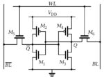
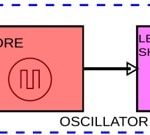
Every year EDA vendor MunEDA hosts a user group meeting where engineers present how they used automation tools to improve their IC designs, and one presentation from Peter Huber of Infineon caught my attention, it was all about SRAM design optimization. Peter has authored papers at IEEE conferences and been issued patents related… Read More
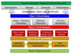
The MunEDA User Group Meeting (MUGM) has been an annual event since 2006, and this year there were some 80 participants from many customers that attended to share their experiences and learn how to get the best EDA tool results. I’ve been able to view the presentations and archived videos, so will share some of the interesting… Read More
Russell Mohnis the Co-Founder and Director of RF/AMS Design at InPlay Inc. and his team has been using WiCkeD from MunEDA for several years. We thought the rest of the world would like to learn about his experiences.
How did you get started in semiconductors and what brought you to InPlay?
I was initially drawn to analog and mixed-signal… Read More
Analog IC designers can spend way too much time and effort re-using old, familiar, manual iteration methods for circuit design, just because that’s the way it’s always been done. Circuit optimization is an EDA approach that can automatically size all the transistors in a cell, by running SPICE simulations across… Read More
My IC design career started out with manually sizing transistors to improve performance, while minimizing layout area and power consumption. Fortunately we don’t have to do manual transistor sizing anymore, thanks to EDA tools that are quicker and more accurate than manual methods. MunEDA is an EDA vendor that has developed… Read More
It has been my pleasure to interview Harald Neubauer, CEO of MunEDA. A veteran of the EDA industry, Harald cofounded MunEDA in 2001.
What brought you to the EDA industry?
Well, I always wanted to found a tech startup and was developing and evaluating various business ideas together with my later cofounder Andreas. Soon after we got… Read More
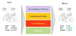
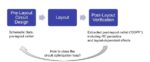
Every year at DAC, in addition to the hubbub of the exhibit floor and the relatively short technical sessions, there are a number of tutorials that dive in depth into interesting topics. At the 56th DAC in Las Vegas this year, MunEDA offered an interesting tutorial on Analog IP migration and optimization. This is a key issue for large… Read More
Configurable analog IP has traditionally been a tough nut to crack. Digital IP, of course, now provides for wide configurability for varying applications. In the same way that analog design has remained less deterministic as compared to digital design, analog IP has also tended to be less flexible. However, the tide may be turning… Read More
When I hear the phrase “high sigma” I think of the EDA vendor Solido, however at DAC on Monday I visited another EDA company called MunEDAthat has several products of interest to transistor-level IC designers. I was able to speak with three different people from MunEDA and here’s what I learned.… Read More
In 2002, MunEDA was launched under the guidance of EDA academic veterans and IEEE fellows Prof. Kurt Antreich and Prof. Helmut Gräb (TUM Munich Technical University ) which represented 20 plus years of EDA research and experience. All MunEDA tools are combined in a tool suite called WiCkeD[SUP]TM[/SUP]. The tool suite brand was… Read More