You are currently viewing SemiWiki as a guest which gives you limited access to the site. To view blog comments and experience other SemiWiki features you must be a registered member. Registration is fast, simple, and absolutely free so please,
join our community today!
A long standing tradition has returned to EDA: The CEO Outlook sponsored by ESDA (formerly EDAC) which alone is worth the price of membership! Not only do you get a free meal, the event included quality networking time with the semiconductor elite. In the past, financial analysts moderated this event holding the CEO’s feet to the… Read More
Back in the day the Dracula tool from Cadence was king of the DRC and LVS world for physical IC verification, however more recently we’ve seen Calibre from Mentor Graphics as the leader in this realm. Cadence wanted to reclaim their earlier prominence in physical verification so they had to come out with something different… Read More
The EDA & IP industry enjoys high growth for the Design IP segment, but a detailed analysis tool is missing. IPnest will address this need in 2017, expecting the IP vendors’ contribution! If we consider the results posted last March by the ESD Alliance, the EDA (and IP) industry is doing extremely well, as the global revenue has… Read More
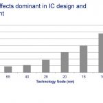
As feature sizes have shrunk, the semiconductor industry has moved from simple, single-exposure lithography solutions to increasingly complex resolution-enhancement techniques and multi-patterning. Where the design on a mask once matched the image that would be produced on the wafer, today the mask and resulting image … Read More
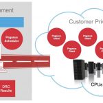
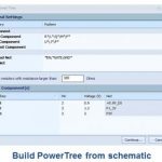
The difficulty of managing the power domains on a complex SoC led to the development of a power format file description, to serve as the repository for data needed for functional and electrical analysis (e.g., CPF, UPF). Yet, what about complex printed circuit boards? How can the power domain information be effectively represented… Read More
It will soon be 20 years since ClioSoft started its journey of selling design management software for the semiconductor industry. It was a slow start considering that designs were relatively small and only digital front-end designers had begun to realize the importance of version control and design management. With open source… Read More
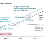
I’ll never forgot working at Intel on a team designing a graphics chip when we wanted to simulate to ensure proper functionality before tapeout, however because of the long run times it was decided to make a compromise to speed things up by reducing the size of the display window to just 32×32 pixels. Well, when first silicon… Read More
A couple weeks ago I gave a heads-up about a webinar that was being hosted by ClioSoft, Qorvo and Keysight. The topic of the webinar was how to manage custom RF designs across multiple design teams and CAD flows. The webinar was held on February 1st and included presentations by Marcus Ray of Qorvo and Michele Azarian of Keysight.
Much… Read More
Bluetooth has been very successful for many years, but arguably trapped in a niche, at least for us consumers, as a short-range wireless alternative to a wire connection – to connect your phone to a car or speakers for example. (In fairness I should add that the 4.2 version has improved range and Bluetooth has already become quite … Read More
Every year certain technology themes appear, like at ITC this year a big theme was how to reduce the cost of SoC testing. I spoke with Rob Knoth of Cadence by phone to hear more about this cost of test theme. Rob gave me an example of an SoC that takes 27 seconds on a tester, so at $0.04 per second in test costs amounts to $1.08 per part. If you… Read More