There has been a lot of new information available about the leading-edge logic processes lately. Papers from IEDM in December 2017, VLSIT this month, the TSMC and Samsung Foundry forums, etc. have all filled in a lot of information. In this article I will summarize what is currently known.
Process Metrics
Standard cells are used to design logic circuits and the size of standard cells is determined by Contacted Poly Pitch (CPP), Metal 2 Pitch (M2P) and Tracks (number of M2P in the cell height). See figure 1.
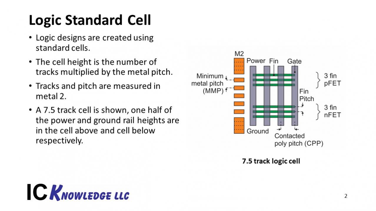
Figure 1. Standard Cell.
In practical cells the use of single diffusion break (SDB) and double diffusion break (DDB) along with CPP determines the actual cells width.
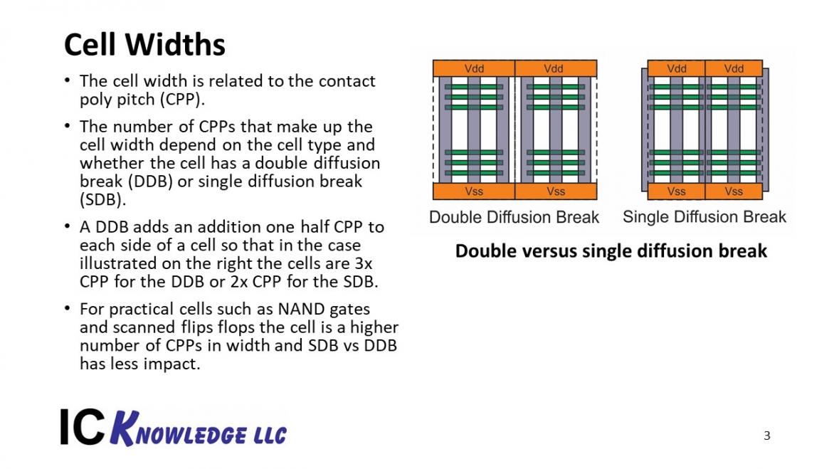
Figure 2. Double Versus Single Diffusion Break.
In cells like a two input NAND gate or Scanned Flip Flops the width in multiples of CPPs is 3 to 4 for SDB/DDB and 19 to 20 for SDB/DDB respectively.
To characterize process density, we use three metrics:
[LIST=1]
7nm
GLOBALFOUNDRIES (GF) disclosed their 7nm dimensions to SemiWiki last year in an exclusive interview available here and discussed their 7LP process at IEDM in December. Intel disclosed the dimensions of their 10nm process at IEDM in December. You can see our GF versus Intel IEDM comparison here. TSMC disclosed some dimensions at IEDM in 2016 and then additional details have come out over the last two years. Samsung was the company with the least available process information but between their recent foundry forum and the teaser available for their VLSIT paper next week the dimensions are now known. Figure 3 summarizes the “7nm” processes, we have included Intel 10nm in the analysis because it is similar in density to the competing “7nm” processes.
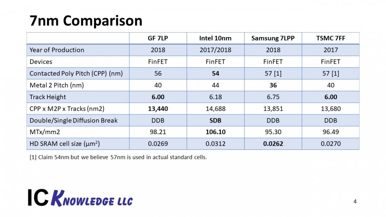
Figure 3. 7nm Process Comparison.
From figure 3 the 4 processes have similar overall process density. GF has the smallest CPP x M2P x Tracks, Intel has the highest MTx/mm[SUP]2[/SUP] value and Samsung has the smallest SRAM cell size. The size of a design in each of these processes will therefore be design dependent and I would not judge any of the four processes to be significantly denser than the others. In terms of relative performance, we have no way to judge that currently.
5nm
The following is a summary of what we currently know about 5nm plans:
- The new CEO of GF Tom Caulfield recently commented that GF is looking for a partner for their next Fab and he said 5nm is probably not enough and they may need to go to 3nm. In an interview I held with GF CTO Gary Patton, Gary wouldn’t put a number on the next node but said it would be full node scaling and a new device. Based on these comments I believe GF’s next process will be a “3nm class” process when you look at the modest scaling planned by Samsung at 5nm.
- Intel’s next node is 7nm due in 2020. During their recent earnings conference, Intel said it would be 2.4x scaling from 10nm.
- Samsung at their foundry forum said that 5nm will have the same pitches as 7nm but switch to SDB and a 6-track cell.
- TSMC on their earnings calls has said 5nm will be 1.9x scaling from 7nm.
Based on this information we have projected 7nm for Intel and 5nm for Samsung and TSMC. Samsung and TSMC will be FinFET based processes. Due to the aggressive scaling Intel is employing we believe they may have to use a Horizontal Nano Sheet (HNS) for their 7nm process. Figure 4 summarizes our projections for the 3 processes.
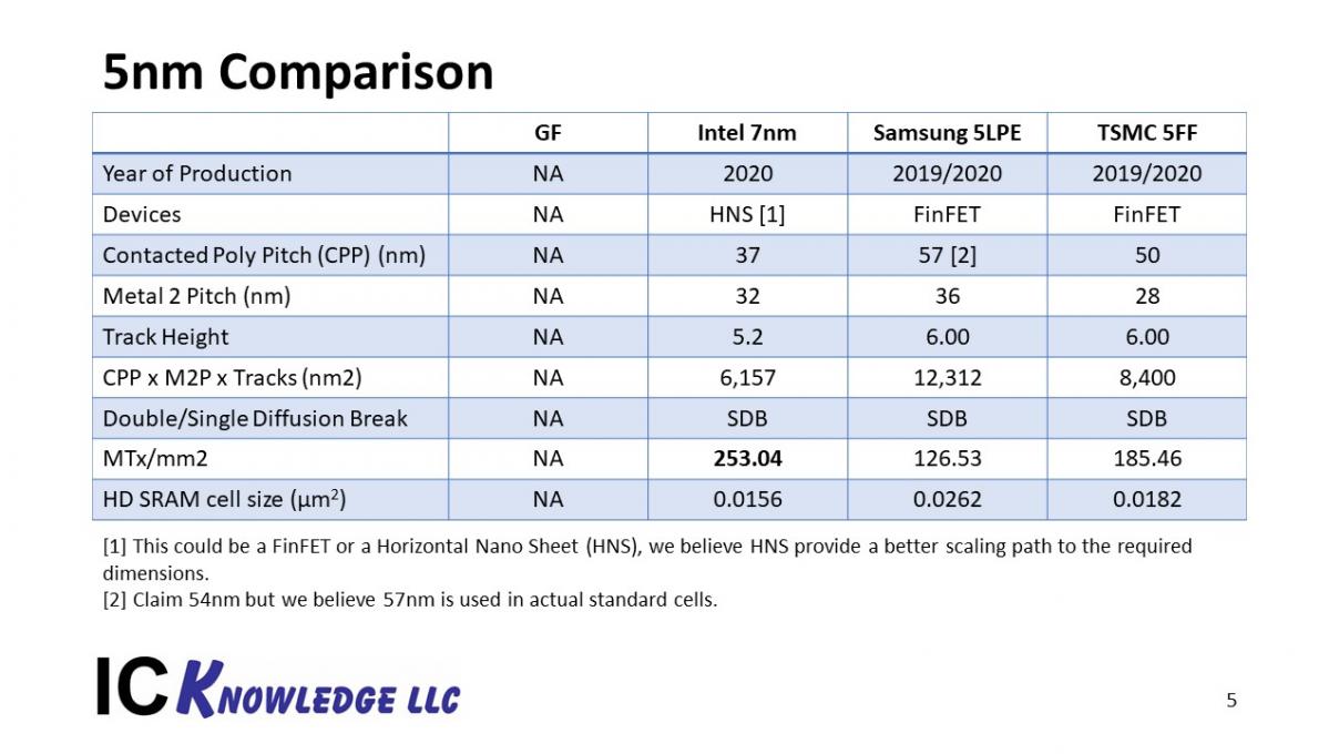
Figure 4. 5nm Process Comparison.
For Intel we developed the process based on 2.4x scaling of MTx/mm[SUP]2[/SUP], we used 32nm for M2P because we believe that is a reasonably achievable EUV pitch for metal. The CPP of 37nm is based on a buildup of the minimum achievable HNS CPP, it is certainly possible the CPP could be larger for performance reasons and the M2P smaller, but that would lead to high interconnect resistance that may be problematic for Intel’s microprocessors. We assumed SDB and scaled the tracks to reach 2.4X.
For Samsung we know the 7nm pitches and we merely changed to SDB and reduced the tracks to six based on the disclosed values.
For TSMC we are hearing they are aggressively scaling M2P so we relaxed CPP, stayed at 6 tracks and went to SDB to get 1.9x scaling. The higher interconnect resistance would likely be less of an issue for mobile applications.
One thing that stands out in figure 4 is that Samsung’s scaling is modest, and Intel’s is very aggressive. In my opinion Intel’s aggressive scaling could lead to a delayed process at 7nm much the same as we have seen at 14nm and 10nm.
3nm
Further projecting to 3nm becomes more speculative.
I have assumed GF and Samsung use a relaxed 45nm CPP with HNS and a reasonable 32nm M2P. Samsung has announced HNS for this node and based on the new device comments from GF I am expecting they will go with HNS as well. HNS also help with track scaling so I have assumed 5 tracks and SDB for both companies.
For TSMC I have assumed 28nm M2P the same as the 5nm process and a CPP shrink to 45nm based on HNS.
Figure 5 compares the three foundry 3nm processes to Intel’s 7nm processes.
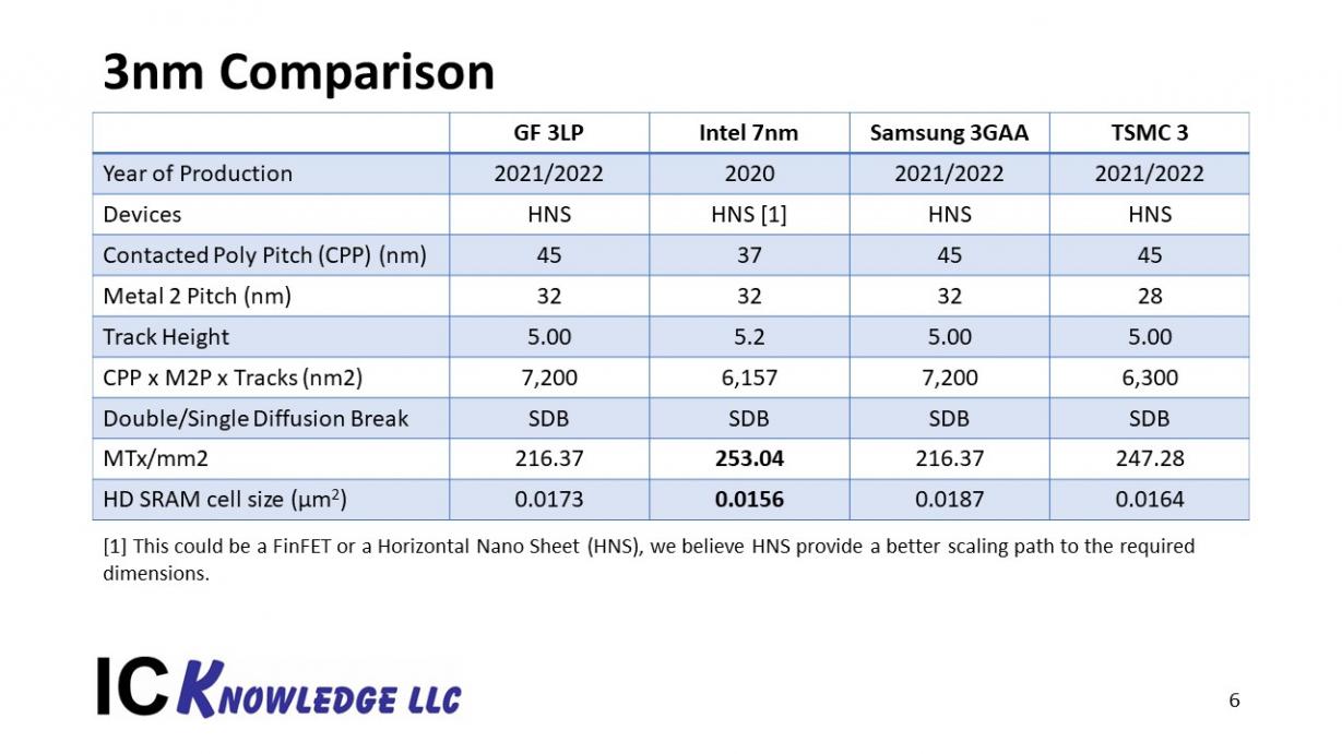
Figure 5. 3nm Process Comparison.
The interesting result is that only TSMC approaches Intel’s 7nm density once again highlighting how aggressive Intel’s plans are.
Discussion
There appear to be two schools of thought on process scaling, Intel and to a lesser extent GF are now producing less frequent but more aggressively scaled processes. Samsung and TSMC are producing more frequent processes but with smaller shrinks (Samsung also has a 4nm process planned that isn’t discussed here).
At the 7nm (foundry)/10nm (Intel) all four companies have similar process density.
Going forward Intel’s 7nm process appears to line up as denser than foundry 5nm and even appears to match up favorably to foundry 3nm processes.
Interested parties can find all this detail and more as well as detailed cost projections in our Strategic Cost and Price Model available for purchase on our web site here, We are also available for consulting projects on process density and cost.
Share this post via:


Captain America: Can Elon Musk Save America’s Chip Manufacturing Industry?