Imec is one of the premier semiconductor research organizations and at IEDM they presented dozens of papers. I had the opportunity to see several of the papers presented and interview 3 of Imec’s researchers.
Jan Van Houdt, DMTS ferroelectric and exploratory memory
I have had very interesting discussions with Imec researchers about memory trends in the past and I asked to interview an Imec memory expert at IEDM this year. Jan Van Houdt has been Imec’s chief scientist and is now DMTS ferroelectric and exploratory memory. My interview with him wasn’t so much tied to specific Imec papers but rather a general discussion of the state of memory.
DRAM scaling has slowed and is facing very difficult issues. Last year at IEDM Imec presented work on Strontium Titanite (STO) dielectric for DRAM with higher K values that could potentially enable capacitor shrinks. He said they still hadn’t met all the specifications for k value, thickness and leakage and they are still trying to add elements to the films to address this. I asked him what he thought would be the long-term replacement for DRAM and he said they thought they could get Ferroelectric based memories to cost and density parity with DRAM but endurance is the key limiter. I was surprised by this, I thought Ferroelectric based memories were really just a niche memory but he was very optimistic about the future of Ferroelectric memories and that is why he has made it his focus. The current Ferroelectric material of choice is HfZrO4 with an endurance of 1E11 cycles.
Authors notes, DRAM replacement endurance needs to be >1E15 cycles. Of the current emerging memory types only MRAM and Ferroelectric have good endurance, PCRAM and RRAM are <1E8 cycles. MRAM can potentially have very good endurance but the high switching current requires large selector transistors limiting scaling.
If Ferroelectric can’t replace DRAM as main memory it could be a storage class memory option. He noted that 3D XPoint, a current storage class memory option is too expensive for the performance it offers.
With respect to 3D NAND scaling he mentioned that as the number of layers increases in 3D NAND memory, that the channel resistance becomes an issue. Imec has previously presented work on InGaAs as an alternative to the current polysilicon channels to provide lower resistance. In the original work the InGaAs was in direct contact with the ONO (Oxide-Nitride-Oxide) layer and had a bad interface. They are trying high pressure anneals and looking at ALD deposition. Ideally, they want to use ALD to deposit a crystalline channel. There is currently work being done in the industry to provide a crystalline silicon channel in place of the polycrystalline channel, with epitaxial growth or recrystallization being investigated. To-date epitaxial growth is too slow and expensive and NiSi recrystallization is slow and the Ni stays in the wafer.
There is also a lot of work being done to replace the W word line material in 3D NAND with a lower resistance alternative. They are looking at TiN to fix the channel work function and then Ru fill or Ru without TiN, Mo is also on the list. The switch to an alternate material will be driven by the need to reduce the layer thickness.
Authors note, as an expert in fabrication costs I think Ru will be much too expensive to implement in 3D NAND especially since the deposition is surface area driven and the surface area with a hundred or more word line slots to fill is very high and drives a lot of precursor consumption.
Imec has completed their work on STT MRAM and they are now focused on SOT MRAM using VCMA – Voltage Controlled Magnetic Anisotropy to switch without current. STT must run current through the Magnetic Tunnel Junction (MTJ) for reading and writing. SOT has no current through MTJ, you run the current near it to write but still need to run current through the MTJ to read it. SOT is a three terminal device, so bigger but can switch in 300 picosecond giving SRAM speed. They don’t have the endurance yet; it is early to talk reliability. In theory should be better than STT, STT is 1E10 to 1E12 but some bits fail earlier.
In Ferroelectrics they can do a FET that is a NAND cell and can provide thinner layers for 3D NAND. With InGaXOx they can do a 2T1C (2 transistor – 1 capacitor) memory cell for DRAM like memory, it has a very small capacitor because it is amplified can be in the Back End Of Line (BEOL). They can also try 1T1C (current DRAM standard) or 2T0C and use a parasitic capacitance. He thinks 2T1C is the most interesting.
Christopher Wilson, manager, nano interconnect program and BEOL integration
In this interview we discussed the paper: “Three-Layer BEOL Process Integration with Supervia and Self-Aligned-Block Options for the 3 nm Node”
This paper is an extension of work presented at the IITC conference where they showed 2-layer Ru with metal 2 at a 21nm pitch, the new work adds a 3rd metal layer. In order to achieve a 21nm pitch you need 2 block masks and they used self-aligned block. This work was done on a SRAM so it has a regular layout. The addition of metal 3 allows them to look at stacked vias. Landing via 2 on metal 2 is normally a critical design rule for Cu, the yield didn’t change much with island size. With 3 layers they can also look at super vias with a via from M3 to M1. Authors note super vias are when vias skip metal layers so instead of connecting metal n to metal n-1 you can connect to n-2, n-3 or more.
This paper was all based on ALD deposition of Ru, Co CVD deposition showed gaps. They have newer data on CVD of Ru but this is all ALD based. The ALD Ru deps were 3 hours per wafers and topped with PVD so a CVD or faster ALD deposition will be needed for production.
One important layout dimension in routing is the metal line tip to tip dimension that you want as small as possible. For Cu typically tip to tip is the same as the pitch so for a 21nm pitch, the tip to tip would be 21nm. In the paper they show no change in yield for a tip to tip of 18nm versus a tip to tip of 9nm and the 9nm is actually around 5nm. Ru has 30% better RC (Resistance-Capacitance) than Cu at these pitches.
For M3 the pitch is 36nm and that shows a 10x RC improvment versus M2 at 21nm.
Naoto Horiguchi, Director of CMOS device technology
In this interview we discussed four Imec papers.
First up was “Novel forksheet device architecture as ultimate logic scaling device towards 2nm”
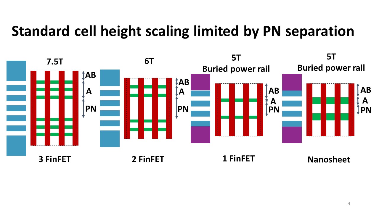
The forksheet is a advanced version of a horizontal nanosheet (HNS) where a dielectric sheet is placed between the nFET and pFET. Because of how HNS are fabricated they can end up with a larger n to p spacing than a FinFET. The additional of the dielectric wall acts as an etch stop layer. Figure 1 illustrates the effect of n to p spacing on standard cell size.

Figure 1. N to P spacing effect on standard cell size.
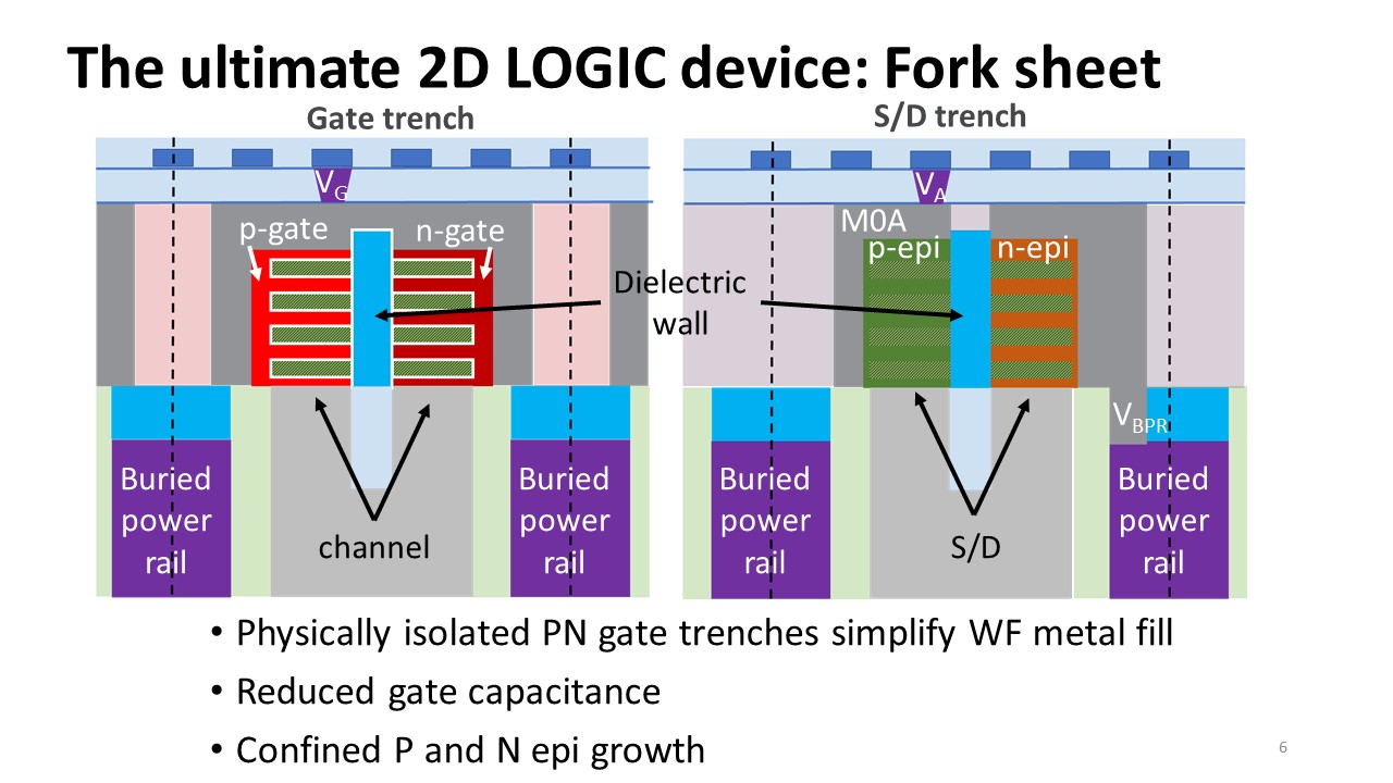
Figure 2 illustrates how a dielectric wall in a forksheet mitigates the n to p spacing.

Figure 2. Forksheet dielectric wall mitigates n to p spacing issues.
A forksheet is essentially a FinFET rotated 90 degrees so the electrostatic are not as good as a standard HNS. Recessing the channel during dielectric wall formation can help recover some electrostatic performance. The dielectric wall reduces miller capacitance and can yield 10% higher speed or 24% lower power.
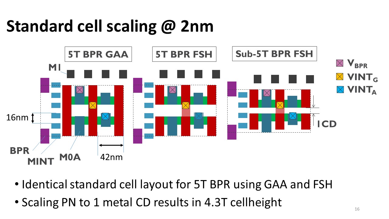
N to p boundary is typically 2x the Fin pitch, the dielectric wall reduces this. For example a 5 track height cell can be reduced to a 4.3 track height cell with the dielectric wall, see figure 3.

Figure 3. Cell scaling advantage for forksheet with dielectric wall.
He believes that the forksheet provides a minimum 20% area improvement.
The second paper we discussed was: “Variability sources in nanoscale bulk FinFETs and TiTaN- a
promising low variability WFM for 7/5nm CMOS nodes”
TiTaN si a potential work function material for controlling threshold voltages (Vt). They deposited it on a high-k dielectric and compared it to TiN and TiN with a SiH4 soak. The SiH4 soak of TiN kind of dopes some silicon atoms on the surface and reduces crystallization improving variability and Vt shift. TiTaN showed a significant further reduction in variability, it is a more amorphous material. TiTaN can be deposited by ALD and can be used on n or p although on p a TaN barrier is needed to block from TiAl.
The third paper we discussed was: “3D-carrier Profiling and Parasitic Resistance Analysis in NW h-GAA CMOS Transistors”
In this work a diamond tipped atomic force microscope is as a scalpel to remove material while also running a spreading resistance probe and create a 3D map of conductivity.
What was found is that dopant diffusion is slow in HNS at the S-SiGe interface.
Authors note, HNS are fabricated as alternating layers of Si and SiGe where the SiGe is a sacrificial layer that gets removed later.
This reduced diffusivity effect will become more important as devices scale and it can impact interface resistance. The ability to measure conductivity at a nanoscale enable better modeling and fundamental understand for future device development.
The final paper we discussed was: “Vertical Nanowire and Nanosheet FETs: Device Features, Novel Schemes for Improved Process Control and Enhanced Mobility, Potential for Faster & More Energy Efficient Circuits”
Vertical nanowires (VFET) are very good for regular layouts such as SRAM or MRAM selectors but not as good as HNS for random logic. This work continues previous Imec work on these devices to further refine the fabrication and performance.
In this work a sacrificial SiGe sleeve is used to introduce stress, the sleeve is fabricated introducing stress and then later removed. This work also showed improved alignment control with a partially self-aligned technique using spacers.
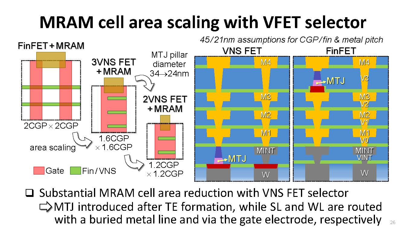
This work could be very interesting for fabrication of highly optimized SRAM chiplets to integrate with logic using 3D packaging techniques. I also found the MRAM selector option very interesting. As I mentioned earlier in this article MRAM selector size is relatively large and limits MRAM scaling. Figure 4 illustrates density improvements by using VFET versus a FinFET.

Figure 4. VFET MRAM selector area advantage versus FinFET.
Conclusion
Imec continues to be a premier research organization in Semiconductor devices and process technology. Innovations such as VFET and Forksheet HNS provide promising options for future scaling. More fundamental work such as understanding carrier profiles in 3D and new work function materials are also key enablers.
Share this post via:


Comments
There are no comments yet.
You must register or log in to view/post comments.