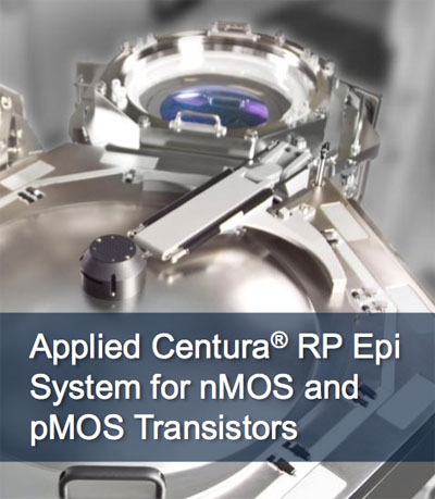
At Semicon I met with Applied Materials to learn about epitaxy. This is when a monocrystalline film is grown on the substrate which takes on a lattice structure that matches the substrate. It forms a high purity starting point for building a transistor and is also the basis of the strain engineering in a modern process.
Since holes have lower mobility than electrons, p-type transistors are inherently lower performance than n-mos transistors (which is why before we had CMOS, semiconductor was dominated by NMOS and its variants, n-type transistors with some sort of pull-up resistor/transistor). Since epitaxy improves performance, it was first used for the p-type transistors.
Basically, the source and drain are etched out to form a pit and then the pit is filled by depositing epitaxial silicon (with Applied Materials equipment in most cases). It is actually deposited until the source/drain is proud of the surrounding silicon. Adding small amounts of impurities that are larger than silicon, such as germanium, during deposition induces strain in the lattice which turns out to enhance mobility in the channel. It increases transistor speed but does so, unlike many other things we might do, without increasing leakage and so without increasing static power.
But now, at 22/20nm nodes, epitaxy is needed to get extra performance out of the n-type transistors too, an contribution of around 20% of the mobility.
As usual, almost anything associated with p-type transistors is the other way around for n-type. So to improve performance, strain needs to be tensile. To induce tensile strain in n-type transistors the impurities need to be smaller than silicon, such as carbon or phosphorous atoms. Carbon is 62% smaller than a silicon atom, for example. This increases electron mobility and thus n-type transistor performance.
There are several advantages of epitaxy especially when it is used for both transistor types:
- precision channel material (since it is not used for source and drain) enhances performance
- physically raised source and drain keep metal contacts away from channel
- increased strain on channel increases drive current
Applied are the leader in equipment for epitaxy having shipped over 500 systems (and more every week). Their revenue in this area increased by 80% over the last 5 years. Looking forward, the market is moving towards new channel materials such as III-V elements which have inherently higher electron mobility.
The bottom line message: nMOS epitaxy is essential for faster transistors inside next-generation mobile processors. It boosts transistor speed by the equivalent of have a device node without increasing off-state power consumption. What’s not to like? That is why it is coming to a 20/22nm process near you.
More details here.
Share this post via:


Comments
There are no comments yet.
You must register or log in to view/post comments.