You are currently viewing SemiWiki as a guest which gives you limited access to the site. To view blog comments and experience other SemiWiki features you must be a registered member. Registration is fast, simple, and absolutely free so please,
join our community today!
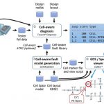
The goal of SoC design teams is to tape-out their project and receive working silicon on the first try, without discovering any bugs in silicon. To achieve this lofty goal requires all types of specialized checking and verification during the design phase to prevent bugs. There are checks at the system level, RTL level, gate level,… Read More
In the earliest days of IC design the engineering work was always done at the transistor-level, and then over time the abstraction level moved upward to gate-level, cell-level, RTL level, IP reuse, and high-level modeling abstractions. The higher levels of abstraction have allowed systems to be integrated into an SoC that can… Read More
During SNUG I took the opportunity to chat to Choon-Hoe Yeoh of Lattice Semiconductor about how they use Concept Engineering’s Starvision Pro product. He is the senior director of EDA tools and methodologies there.
Lattice Semiconductor is a manufacturer of low-power, small-footprint, low-cost programmable logic devices.… Read More
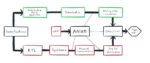
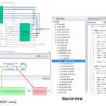
In today’s SoC world where multiple analog and digital blocks along with IPs at different levels of abstractions are placed together on a single chip, debugging at all levels becomes quite difficult and clumsy. While one is working at the top level and needs to investigate a particular connection at an intermediate hierarchical… Read More
RTL designers know that their code gets transformed into gates and cells by using a logic synthesis tool, however these gates and cells are further comprised of transistors and sometimes you really need to optimize the transistor sizing to reach power, performance and area goals. I’ve done transistor-level IC design before,… Read More
So what comes after FinFETs? At 14/16nm (or 22nm if you are Intel) we had FinFET transistors, where the channel was no longer planar but stuck out of the wafer vertically, and the gate wrapped around it on 3 sides. The key thing that made FinFET transistors attractive was that the channel was thin so that the gate controlled it well. … Read More
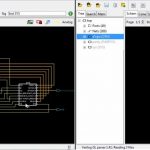
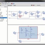
A very popular acronym is ‘WYSIWYG’ – What You See Is What You Get! This is very true and is important to visualize things to make it better in various aspects such as aesthetics, compactness, organization, structure, understandable for correction and so on; the most important, in case of semiconductor design, is being able to identify… Read More
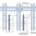
When we talk about parasitic, we talk about post layout design further expanded in terms of electrical components such as resistances and capacitances. In the semiconductor design environment where multiple parts of a design from different sources are assembled together into highly complex, high density SoC, imagine how complex… Read More
At Semicon I met with Applied Materials to learn about epitaxy. This is when a monocrystalline film is grown on the substrate which takes on a lattice structure that matches the substrate. It forms a high purity starting point for building a transistor and is also the basis of the strain engineering in a modern process.
Since holes… Read More
In the last few decades, electronics has become more and more central to our lives. When I was a child the only electronics in the house was the radio and the television, both of which contained tubes. Two big things happened that upended that world: the invention of the transistor and the invention of the integrated circuit. A modern… Read More