I have seen several articles recently discussing foundry wafer selling prices for leading edge wafers, these articles all quote estimates from a paper by the Center for Security and Emerging Technology (CSET). The paper is available here.
My company IC Knowledge LLC is the world leader in cost and price modeling of semiconductors and MEMS. We have been selling commercial cost and price models for over twenty years and our customer base is a who’s who of system companies, fabless, foundries and IDMs, OEMS, materials companies and analysts. I thought it would be interesting to examine how the estimates in the paper were produced and how realistic they are.
Capital Costs
CSET begins their analysis looking at TSMC’s financial releases and find from 2004 to 2018 that revenue can be broken down into 24.93% depreciation, 36.16% other costs and 35.91% operating profit. They also come up with a 25.29% capital depreciation rate. They then go on to calculate capital consumed per wafer and then use these percentages to infer other costs. I see a couple of problems with this approach, one, it assumes these ratios are the same for all nodes, they aren’t, and two, the depreciation rate makes no sense as I will explore further below.
The capital consumed calculation is as follows:
“To obtain capital consumed per wafer, we first calculate capital investment per wafer processed per year. TSMC currently operates three GigaFabs (Fabs 12, 14, and 15) with a fourth (Fab 18) scheduled to come online in 2020 with expansion thereafter.”
This ignores TSMC’s Fab 16 with two phases in China.
“These four fabs include a total of 23 fab locations each with a known initial capital investment in 2020 USD— representing investments in facilities, clean rooms, and purchase of SME—and annual 300 mm wafer processing capacity.”
Fabs 12, 14 and 15 are each 7 phases, Fab 18 is planned to be 6 phases, apparently they are considering the 21 phases from Fabs 12, 14, and 15 plus 2 phases from Fab 18 that have recently come on-line and ignoring Fab 16 (although Fab 16 is relatively small and therefore less significant than the GigaFabs).
They plot capital investment per 300mm wafer processed per year and fit an exponential trend line to the plot.
I do not know what their specific data source is, TSMC sometimes announces fab capacity and initial investment but not always and these are often more aspirational numbers than actual costs. These fabs also often have an initial cleanroom build and then are equipped over time as they are ramped up with ramps covering more than one year. The ultimate fab capacity is often the result of additional investments. It is not clear to me how this becomes a cost per wafer per year with this approach. These values eventually get converted to capital investment per wafer per year by node based on the year and quarter each node was introduced and then assuming the capital investment per wafer by year represents that node. The problem is TSMC is not always only ramping one node in any given year plus the other issues discussed above.
The way we address capital cost in our models is fundamentally different and more detailed.
- For each node we built a representative process flow, this is done based on our own experience, consultation with industry experts, conference papers, patents, and actual construction analysis from our strategic partner TechInsights.
- We maintain a database of every 300mm wafer fab in the world tracking the initial and all upgrade states. This database is a combination of public and private sources.
- We maintain a database of equipment throughput, cost and footprint by node and wafer size. Once again this is based on public and private sources. Our Strategic Cost and Price Model is in use at all the major equipment OEMs and we have an extensive network of sources for this information.
- For each 300mm fab we calculate a fab size and cost and equipment set based on the specifics of the process, and the fab states. We calculate this for the initial fab state and up to twelve upgrades or expansions per fab.
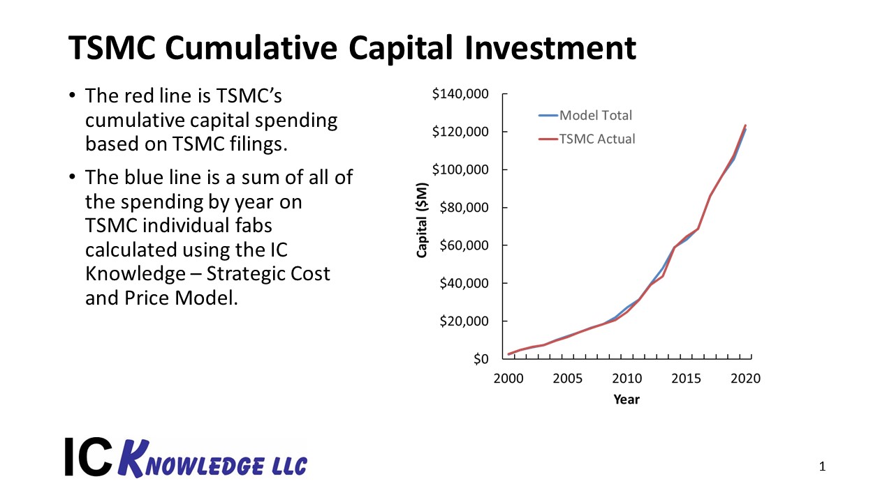
With the amount of information going into these calculations and the complex methods used we need to validate our methods. Around 2000 – 300mm fab began to come on-line and quickly accounted for most of the capital spending at all the major semiconductor companies. For TSMC as an example, we have taken their publicly disclosed capital spending each year since 2000 and plotted it versus year as a cumulative number. We have then modeled all their 300mm fabs and spending by fab by year and added that up to create a cumulative plot. After accounting for some residual 200mm spending in the early years and any spending not yet on-line (our spending calculations are based on on-line dates) we get the following plot.

Figure 1. TSMC calculated versus actual cumulative capital spending.
The resulting plot shows excellent match. We have done this same analysis for Samsung, Intel, Micron Technology and many others with equally good correlation.
TSMC typically focuses a fab on a single node so we now have capital costs per wafer-out estimates by node. Comparing our estimates by node to the estimates in row 2 of table 9 in the CSET paper we find that at the 90nm node the values are similar, but they steadily diverge as the nodes get smaller.
In the CSET paper rows 3 and 4 provide a net capital depreciated and undepreciated capital at the start of 2020 that are then used with a 25.29% depreciation rate to get the capital consumed per wafer value presented in row 5. This whole calculation makes no sense to me. TSMC has disclosed they use 5-year straight-line depreciation for equipment and 10-year straight-line for facilities. What this means is that if you put a piece of equipment on-line you write-off 20% of the equipment investment each year for the first 5 years and then the depreciation goes to zero in year 6. For facilities you write-off 10% of the value each year for 10 years and then the depreciation goes to zero. 90nm in 2020 is fully depreciated and even brand new 5nm investment is only depreciating at something less than 20% after blending equipment and facility depreciation.
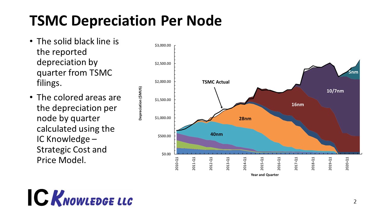
Applying five-year straight-line for equipment, equipment installation and automation and ten-year straight-line depreciation to facilities values from our calculation we get the following depreciation by node plot. Also, on the plot is TSMC’s reported depreciation and as in the previous figure you can see the match is excellent.

Figure 2. TSMC calculated depreciation by node and quarter versus TSMC reported depreciation.
Based on these plots and other comparisons we have made it is clear our capital calculations are highly accurate.
Other Costs and Markup
This bring us to the other elements that add up to revenue.
First, to complete the wafer cost calculation:
- Starting Wafer – starting wafers are purchased from wafer suppliers and we have contacts at wafer brokers and wafer suppliers who provide us with the open market pricing.
- Labor – we have an extensive database of direct and indirect labor rates by country and year built up from a network of private and public sources.
- Equipment maintenance – we use a percentage of the capital investment in equipment to estimate the equipment maintenance cost. The percentage varies depending on wafer size and product type being made in the fab, for example memory is different than logic.
- Facilities – we do detailed facilities operating cost calculation accounting for electric and natural gas rates by country and year and equipment requirements, ultrapure water cost, waste disposal, facilities maintenance, insurance costs, and more. Once again, we have public and private data sources.
- Consumables – based on the process flow we calculate the usage of hundreds of individual consumables and combing that with a database of cost by consumable and year calculate the total consumable costs. We get consumable usage and cost data from our strategic partner Linx Consulting as well as an extensive network of materials suppliers.
The summation of these values and the depreciation results in manufacturing costs per node.
To get to selling price, a gross margin must be applied where the gross margin includes Selling, General and Administrative Costs (SG&A), Research and Development Costs (R&D) and Operating Profit. TSMC discloses average gross margin in their filings, however gross margin is not flat across their product line (it also varies with fab utilization). When a new process comes on-line, depreciation costs are high but then as the equipment becomes fully depreciated the wafer manufacturing costs drops more than in-half. TSMC and other foundries typically do not pass all the cost reduction that occurs when equipment becomes fully depreciated on to the customer, the net result is that gross margins are lower for newer processes and higher for older fully depreciated processes. We account for this in our calculation, but once again the calculation disclosed in CSET the paper assumes the other wafer costs and gross margin are consistent from node to node.
In our case we have a variety of ways to check our wafer prices including customers who buy wafers and compare them to our calculations, and our ability to use proprietary methods to compare our results to company filings. For example, we have compared our calculated results to TSMC’s filings every quarter from Q1-2000 to Q2-2020 with excellent match every quarter.
This brings us to the key question, how accurate are the row 7 “Foundry sale price per wafer” values in the paper and the answer is not very. There is basically an error slope to the results with the 90nm prices being too low and at 5nm the prices are too high.
Conclusion
Although the value in the CSET are not off by an order of magnitude, they are off. I have customers frequently ask me for rules of thumb and I tell them my rule of thumb is that all rules of thumb are wrong. Accurate estimates of wafer manufacturing costs and selling prices require detailed calculations such as are embodied in our commercial cost and price models. We currently offer five cost and price models targeting different segments of the semiconductor and MEMS industries.
For more information on our models please go to www.icknowledge.com
Also Read:
VLSI Symposium 2020 – Imec Monolithic CFET
SEMICON West – Applied Materials Selective Gap Fill Announcement
Imec Technology Forum and ASML
Share this post via:


Comments
8 Replies to “Leading Edge Foundry Wafer Prices”
You must register or log in to view/post comments.