Even though this is the 16th OIP event please remember that TSMC has been working closely with EDA and IP companies for 20+ years with reference flows and other design enablement and silicon verification activities. The father of OIP officially is Dr. Morris Chang who named it the Grand Alliance. However, Dr. Cliff Hou is the one who actually created the OIP which is now the largest and strongest ecosystem in the history of semiconductors.
I spent a good portion of my career working with EDA and IP companies on foundry partnerships as well as foundries as a customer strategist. In fact, I still do and it is one of the most rewarding experiences of my career. Hsinchu was my second home for many years and the hospitality of the Taiwan people is unmatched. That same hospitality is a big part of the TSMC culture and part of the reason why they are the most trusted technology and capacity provider.
Bottom line: If anyone thinks this 20+ years of customer centric collaboration can be replicated or reproduced, it cannot, the OIP is a moving target, it expands and gets stronger every year. An ecosystem is also driven by the success of the company and in no part of history has TSMC been MORE successful than today, my opinion.
We will be covering the event in more detail next week but I wanted to share my first thoughts starting with a quote from a blog published yesterday by Dan Kochpatcharin, Head of Ecosystem and Alliance Management Division at TSMC. I met Dan 20 years ago when he was at Chartered Semiconductor. For the last 17 years he has been at TSMC where he started as Deputy Director of the TSMC IP Alliance (working for Cliff Hou) which is now a big part of the TSMC OIP.
Advancing 3D IC Design for AI Innovation by Dan Kochpatcharin
“Our collaboration with TSMC on advanced silicon solutions for our AWS-designed Nitro, Graviton, Trainium, and Inferentia chips enables us to push the boundaries of advanced process and packaging technologies, providing our customers with the best price performance for virtually any workload running on AWS.” – Gary Szilagyi, vice president, Annapurna Labs at AWS
Readers of the SemiWiki Forum will get this inside joke and if you think this quote from AWS is a coincidence you are wrong. C.C. Wei has a very competitive sense of humor!
Dr. L.C. Lu (Vice President of Research & Development / Design & Technology Platform) did the keynote which was quite good. I first met L.C. when he was in charge of the internal TSMC IP group working for Cliff Hou. He is a very smart no nonsense guy who is also a great leader. Coincidentally, L.C. and CC Wei both have P.h.D.s from Yale.
Some of the slides were very similar to the earlier TSMC Symposium slides which tells you that TSMC means what it says and says what it means. There were no schedule changes, it was all about implementation, implementation, and implementation.
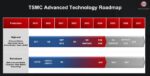
L.C. did an interesting update on Design-Technology Co-Optimization (DTCO). I first heard of DTCO in 2022 and it really is the combination of design and process optimization. I do know customers who are using it but this is the first time I have seen actual silicon results. Remember, this is two years in the making for N3 FinFlex.
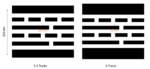
The numbers L.C. shared were impressive. In order to do real DTCO a foundry has to have both strong customer and EDA support and TSMC has the strongest. For energy efficiency (power savings) N3 customers are seeing 8%-20% power reductions and 6%-38% improvement in logic density depending on the fin configuration.
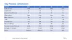
L.C. also shared DTCO numbers for N2 NanoFlex and the coming A16 SPR (Super Power Rail) which were all in the double digits (11%-30%). I do know quite a few customers who are designing to N2, in fact, it is just about all of TSMC’s N3 customers I am told. It will be interesting to see more customer numbers next year.
L.C. talked about packaging as well which we will cover in another blog but let me tell you this: By the end of 2024 CoWos will have more than 150 tape-outs from more than 25 different companies! And last I heard TSMC CoWos capacity will more than quadruple from 2023 levels by the end of 2026. Packaging is one of the reasons why I feel that the semiconductor industry has never been more exciting than it is today, absolutely!
Also Read:
TSMC OIP Ecosystem Forum Preview 2024