





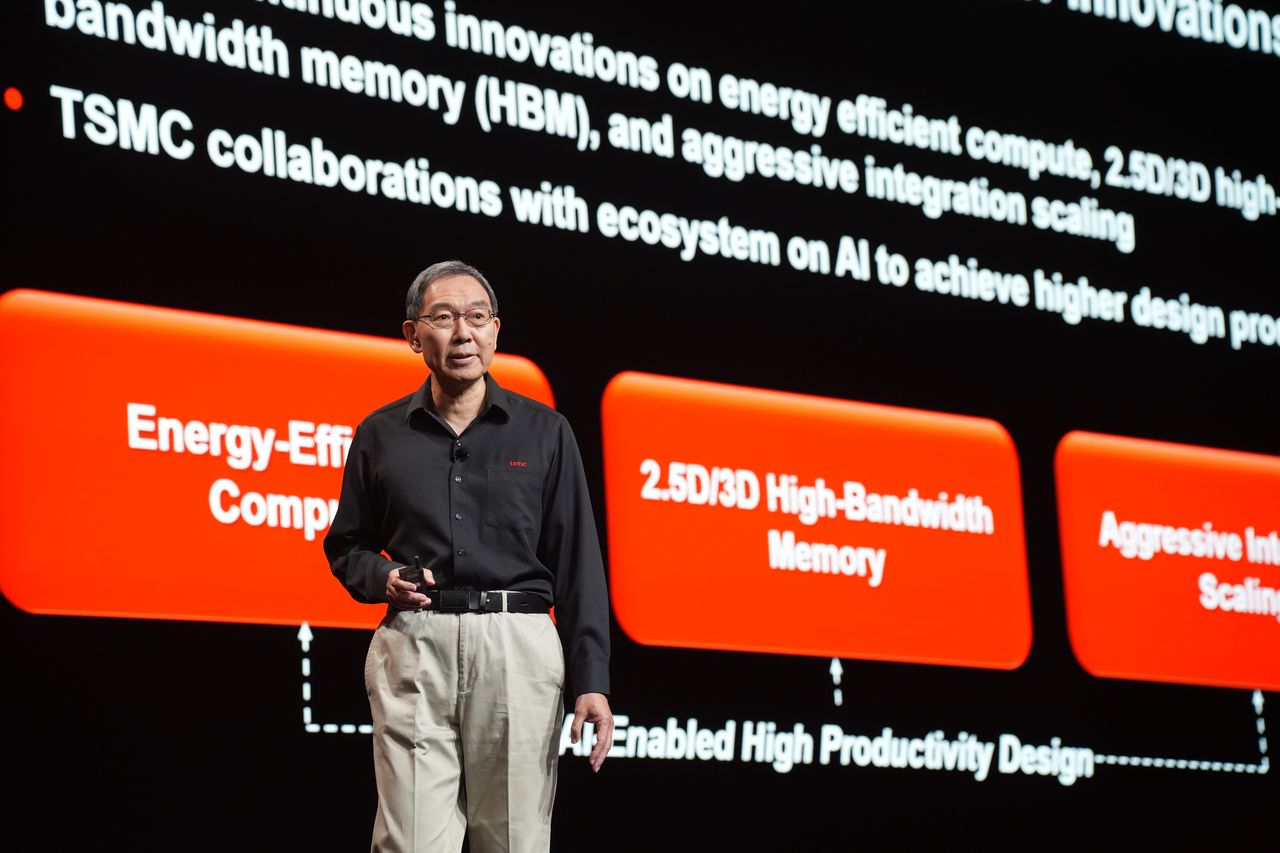
About twenty years ago I worked with Cliff Hou, LC Lu, and the TSMC PDK team on reference flows with emerging EDA and IP companies. This was the precursor to the OIP. Having a person with LC Lu’s depth of R&D experience running the TSMC Design & Technology Platform is truly an honor, absolutely.
AI is creating two related problems for semiconductor designers. They must deliver more computing power for training and inference, while keeping energy use and cost manageable. Dr. LC Lu’s presentation at the TSMC Open Innovation Platform Forum describes a response built around more efficient transistors, closer integration of logic and memory, larger multi-chip packages, optical connections, and AI-assisted chip design.
The central challenge is useful work per unit of energy. An AI system’s cost is shaped not only by how quickly its processors calculate, but also by how much power they draw and how efficiently they receive data. Training a model requires immense computation. Serving that model to users adds a different burden: every generated token consumes processing, memory access and communication capacity. As inference use grows, small improvements in energy per token can have large effects across a data center.
The first part of TSMC’s approach is continued process improvement. New semiconductor processes can improve power, performance and area, the three measures commonly shortened to PPA. The presentation discusses nanosheet transistors and design technology co-optimization, in which engineers adapt circuit design and manufacturing technology together. A transistor alone does not determine a chip’s efficiency. Standard-cell layouts, wiring, placement and the demands of a particular workload all affect the result. TSMC has described its NanoFlex family as giving designers choices that help balance performance and energy efficiency.
Those choices matter because AI hardware is not uniform. A component designed for maximum speed may justify a different circuit layout from one designed for lower power or smaller area. Even within a single system, designers may use different kinds of cells where speed is critical and where it is less important. This is a practical limit on any simple claim that a newer manufacturing process will automatically make every AI workload cheaper: designers still have to turn the process’s capabilities into a working product.
The second part of the roadmap moves beyond the individual chip. AI processors need to exchange enormous amounts of data with high-bandwidth memory, or HBM. If computation becomes faster while memory access does not, processors can spend time waiting for data. Placing memory close to compute through advanced packaging increases the bandwidth available between them and can reduce the energy needed to move each bit. The presentation discusses a hierarchy of memory technologies rather than one universal replacement, reflecting different trade-offs in capacity, bandwidth, latency and power.
Advanced packaging also lets designers combine multiple computing dies in one system. TSMC’s CoWoS technology is an example of this approach, while its 3DFabric portfolio includes three-dimensional stacking. The attraction is scale: engineers can bring together more logic and memory than would fit comfortably on one conventional die. The difficulty is that package size, electrical connections, heat removal, power delivery, testing and manufacturing yield all become system-level design problems. TSMC’s 2026 forum materials place 3DFabric and advanced packaging alongside its leading-edge processes as essential parts of future AI design.
As systems grow, communication between them becomes another constraint. The presentation points to TSMC-COUPE, its compact optical engine, as a path toward high-bandwidth, energy-efficient networking. Optical links use light to carry information and may help where electrical links become costly in power or difficult to scale over distance. This does not mean every wire inside a chip disappears. It means designers are looking for the right connection at each level—from circuitry within a die to communication between large AI systems. TSMC lists co-packaged optics among the technologies featured at its 2026 forum.
The presentation’s other major theme is design productivity. More elaborate processes and packages create more decisions for engineers and more conditions their designs must satisfy. Electronic design automation, or EDA, tools already help turn a circuit plan into a physical layout and check whether it can be manufactured. The presentation describes a proposed AI-oriented design enablement kit and agent-based workflows that could help optimize placement and routing, identify and fix design-rule violations, migrate existing designs, and translate descriptions of three-dimensional chip architectures into a standard design format.
These are consequential tasks, but automation must be judged by the quality of the finished design, not only by how quickly a tool produces an answer. A proposed change still has to meet electrical, thermal, timing and manufacturing requirements. An AI agent may generate options and run repeated tool flows around the clock; engineers and verified design tools must establish that the result works. TSMC describes autonomous AI workflows with its ecosystem partners as a focus of the 2026 forum, while its established Open Innovation Platform brings together design tools, intellectual property and manufacturing guidance.
Shared design descriptions matter in this setting. LC Lu discusses 3Dblox as a way to describe complex multi-die architectures so that different tools and organizations can work from consistent information. TSMC previously introduced 3Dblox for three-dimensional chip design, with the goal of improving interoperability among design tools. For a package assembled from several dies, that common representation can reduce the risk that teams make incompatible assumptions about connections or physical arrangement.
Bottom line: AI progress increasingly depends on improving a whole computing system, not merely making one processor faster. Memory bandwidth, package integration, networking, energy supply and the time needed to design and validate a product can each become the limiting factor. TSMC’s presentation describes these constraints as connected engineering problems: improve the silicon, bring components closer together, move data more efficiently and help designers manage the resulting complexity.
Also Read:
The Intelligence Revolution: TSMC’s OIP Ecosystem Forges the Path to Trillion-Transistor AI Systems
Podcast EP368: An Overview of TSMC Open Innovation Platform (OIP) event with Aveek Sarkar
Comparison of TSMC CoWoS-S, CoWoS-R, and CoWoS-L
TSMC’s CoWoS Capacity to Double by 2028—and Rivals Will Still Win Orders
Share this post via:



Comments
There are no comments yet.
You must register or log in to view/post comments.