FinFETs are hot, carbon nanotubes are cool, and collaboration is the key to continued semiconductor scaling. These were the main messages at the 2013 Common Platform Technology Forum in Santa Clara.
The collaboration message ran through most presenations, like the afternoon talk by Subi Kengeri of GLOBALFOUNDRIES and Joe Sawicki… Read More
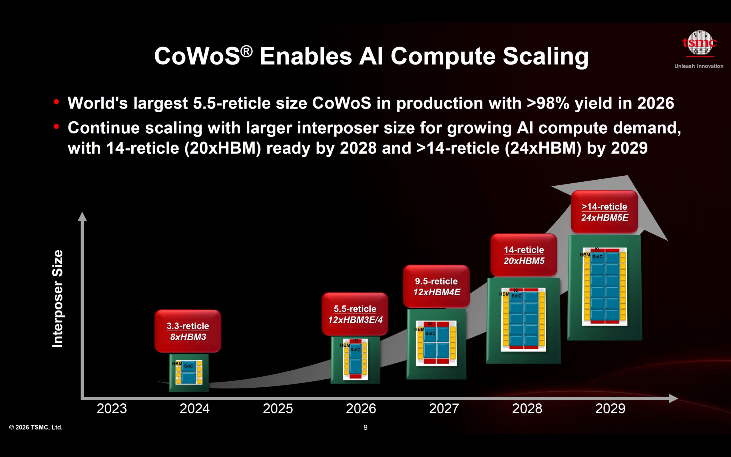 Enabling Next-Generation AI Through Advanced Packaging and 3D Fabric IntegrationThe rapid rise of artificial intelligence is fundamentally…Read More
No EUV before 7nm?
I was at the Common Platform Technology Forum this week. One of the most interesting sessions is IBM’s Gary Patton giving an overview of the state of semiconductor fabrication. Then, at lunchtime, he is one of the people that the press can question. In this post, I’m going to focus on Extreme Ultra-Violet (EUV) lithography.… Read More
Using Soft IP and Not Getting Burned
The most exciting EDA + Semi IP company that I ever worked at was Silicon Compilers in the 1980’s because it allowed you to start with a concept then implement to physical layout using a library of parameterized IP, the big problem was verifying that all of the IP combinations were in fact correct. Speed forward to today and our… Read More
Semiconductors Down 2.7% in 2012, May Grow 7.5% in 2013
The world semiconductor market in 2012 was $292 billion – down 2.7% from $300 billion in 2011, according to WSTS. The 2012 decline followed a slight gain of 0.4% in 2011. Fourth quarter 2012 was down 0.3% from third quarter. The first quarter of the 2013 will likely show a decline from 4Q 2012 based on typical seasonal patterns and the… Read More
RTL Clock Gating Analysis Cuts Power by 20% in AMD Chip!
Approximately 25% of SemiWiki traffic originates from search engines and the key search terms are telling. Since the beginning of SemiWiki, “low power design” has been one of the top searches. This is understandable since the mobile market has been leading us down the path to fame and fortune. Clearly lowering the… Read More
UVM: Lowering the barrier to IP reuse
One of my acquaintances at Intel must have some of the same viewing habits I do, based on a recent Tweet he sent. He was probably watching “The Men Who Built America” on the History Channel and thinking as I have a lot recently about how the captains of industry managed to drive ideas to monopolies in the late 1800s and early 1900s.
… Read MoreDifference
Could “Less than Moore” be better to support Mobile segment explosion?
If you take a look at the explosion of the Mobile segment, linked with the fantastic world-wide adoption of smartphone and media tablet, you clearly see that the SC industry evolution during –at least- the next five years will be intimately correlated with the mobile segments. Not really a surprise, but the question I would like … Read More
Sanjiv Kaul is New CEO of Calypto
Calypto announced that Sanjiv Kaul is the new CEO. I first met Sanjiv many years ago when he was still at Synopsys when I interviewed for a position there around the time I transitioned out of Compass and went back to the parent company VLSI. I forget what the position was. Then about three or four years ago when I did some work for Oasys… Read More
Software Driven Power Analysis
Power is a fundamentally hard problem. When you have finished the design, you have accurate power numbers but can’t do anything about them. At the RTL level you have some power information but it is often too late to make major architectural changes (add an offload audio-processor, for example). Early in the design, making… Read More
Help, my IP has fallen and can’t get up
We’ve been talking about the different technologies for FPGA-based SoC prototyping a lot here in SemiWiki. On the surface, the recent stories all start off pretty much the same: big box, Xilinx Virtex-7, wanna go fast and see more of what’s going on in the design. This is not another one of those stories. I recently sat down with Mick… Read More


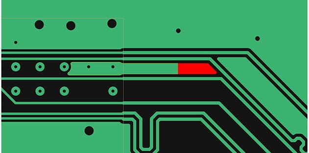






Solving the EDA tool fragmentation crisis