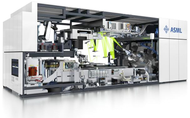
 I was at the Common Platform Technology Forum this week. One of the most interesting sessions is IBM’s Gary Patton giving an overview of the state of semiconductor fabrication. Then, at lunchtime, he is one of the people that the press can question. In this post, I’m going to focus on Extreme Ultra-Violet (EUV) lithography.
You probably know that the biggest challenge is the light source. This is actually made with droplets of tin. One laser shapes the drop and then another high powered laser zaps the drop to create plasma and EUV light. This is collected, goes through 6 mirrors with very low efficiency and a reflective mask. Very little, maybe 5%, of the original light actually makes it to the wafer to expose the photoresist. Right now the power of the light source is up to about 30W but it needs to be more like 250W and so it is off by a factor of 10.
Gary also mentioned two other problems that I’ve written about before but which don’t get mentioned nearly so much. After all, these are only problems if we get a usable EUV light source that works reliably ten billion times a day with adequate power.

The two other problems are that masks will not be defect free and that it is not possible to put a pellicle on the mask (since it would absorb all the EUV).
First, the defect problem. There are two issues. Firstly, the mask will have defects that will print and so either the design needs to be redundant enough that it doesn’t matter or else the defects need to be on parts of the mask that don’t matter since they are going to print anyway. This means knowing where the defects are and that is the next problem. You can’t just look for them with visible light since they are too small. So you need to scan them. But the scale of a mask versus the scale of a defect is huge: it is equivalent to searching 10% of California to make sure there are no golf balls there.
In refractive optics (what we use today) the mask is covered with a thin transparent film called a pellicle. One purpose of the pellicle is that any contamination that would end up on the mask instead ends up on the pellicle. It is thus out of the focal plane of the stepper and so doesn’t print. EUV masks cannot have a pellicle. But that means that any contamination will print. Worse, it won’t be obvious that this his happening and it will continue to print until the mask is cleaned. This is potentially very expensive since hundreds more fabrication steps may take place on a wafer that is actually already a dud. The whole wafer. Every die.
Some people have said that getting EUV to work is “just engineering.” Gary says this is not the case. “It is not just hard engineering work, it is hard physics problems too.” At lunch someone asked Gary if it was like 80% engineering with 20% of physics problems to be resolved. He said he wasn’t really sure how you put a number on it like that but his guess would be 60% physics problems and 40% engineering.
If EUV becomes workable, IBM thinks that it will be for the 7nm node. Not 14nm or 10nm. It seems that “EUV will eventually work because it has to.” But reality doesn’t always cooperate on that basis.
Share this post via:


Is Intel About to Take Flight?