
We’ve been talking about the different technologies for FPGA-based SoC prototyping a lot here in SemiWiki. On the surface, the recent stories all start off pretty much the same: big box, Xilinx Virtex-7, wanna go fast and see more of what’s going on in the design. This is not another one of those stories. I recently sat down with Mick Posner of Synopsys, who led off with this idea:
Design flow is not just about dropping everything in the SoC – or the FPGA-based prototyping system – and seeing what works.
Yet, it seems to be the prevailing thinking: if the FPGA-based prototyping system is massive enough, and we pour all the RTL into it, and manage the partitioning and debugging, we can get an entire SoC running in no time. Not so fast. Let’s step back and look at what we’re trying to do, and where IP falls down in the process.
We’ve been sharing the deepest, darkest fear of the EDA world for a while now. An individual team puts best brains to work on a new IP block, develops requirements, lays in functionality, does some testing, and comes out with something they think is good. They pass it on to an SoC team to incorporate in a design, and all hell breaks loose, and the finger pointing starts. Why do we play this game over and over?
Posner offers a simple explanation, saying that most timing closure issues crop up around external I/O constraints, which are difficult to accurately model and test unless everything that affects the IP block in an SoC design is connected and active at-speed. An IP block team could certainly build experience, for instance using an FPGA-based prototyping system with a known-good SoC design and incrementally adding or replacing just their new block, and then feeding the new block forward into a new SoC design for further testing.
Maybe more importantly, Posner points out there are multiple ways to deliver IP, and each creates potential stumbling blocks for IP being fed forward.
1) RTL – what could possibly go wrong with source code? The SoC team retraces a lot of the steps the IP team went through, duplicating effort. Worse, if the two teams are using different tools and prototyping platforms, they can get very different results.
2) Encapsulated “physical” – this raises a whole bunch of issues between teams if platforms aren’t common, from clocking to power to software interfaces.
3) FPGA binary – again, if the target FPGA isn’t common, this becomes a non-option.
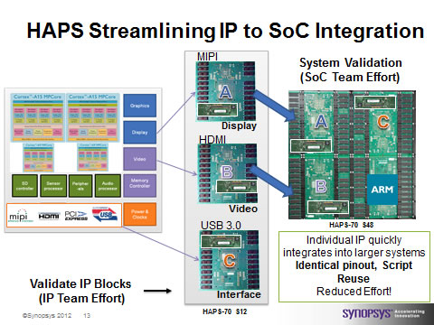
This thinking has gone into the Synopsys HAPS-70 FPGA-based prototyping family, with a common hardware and software architecture from the low end to the high end. The idea is to bring forward an IP block with all the design artifacts: the functional block, scripts, pinouts, timing, and everything so that the IP block is fully represented in all its fidelity on the SoC prototyping system.

The detail in thinking goes right down to the connector level. There are a lot of HapsTrak 3 connector sites on the mainboards, each a 50-pin SEARAY connector. Why so many? The answer lies in the Xilinx Virtex-7, which is a marvelous beast of an FPGA – but it is really composed of four Super Logic Regions. The SLR banks are mapped to connectors, to minimize crossing banks which imposes a huge timing hit compared to intra-SLR timing. If an SoC designer unwittingly spreads a chunk of IP across SLR banks, timing can be thrown way off.
This isn’t a story Posner just cooked up – it comes from listening to FPGA-based prototyping customers, with some obvious and some not-so-obvious problems. His last statement points to the endgame: the Synopsys DesignWare IP teams are starting to implement on HAPS-70, with the exact idea that they create all the pass-forward artifacts fitting into the Certify and Synplify Premier flows so that there is no duplication of effort and greatly improved predictability for an SoC team implementing on a larger HAPS-70.
There is a HAPS-70 webinar coming up on February 6[SUP]th[/SUP] you may want to catch for more info.


Comments
There are no comments yet.
You must register or log in to view/post comments.