You are currently viewing SemiWiki as a guest which gives you limited access to the site. To view blog comments and experience other SemiWiki features you must be a registered member. Registration is fast, simple, and absolutely free so please, join our community today!
On July 30, 2020, NASA launched the Mars 2020 Perseverance rover, which is scheduled to land today. Perseverance has been deployed to Mars with a new mission: to search for evidence of past life and collect samples that will eventually be brought back to Earth by future missions.
Mars 2020 Perseverance rendering courtesy of NASA/JPL-Caltech… Read More
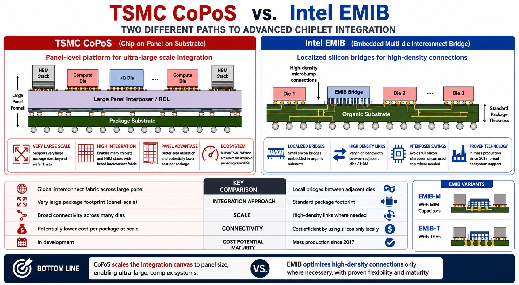
Dan and Mike are joined by Sudhir Mallya, vice president of corporate and product marketing at OpenFive. We explore 2.5D design and the role chiplets play. Current technical and business challenges are discussed as well as an assessment of how the chiplet market will develop and what impact it will have.
Srinath Anantharaman founded Cliosoft in 1997 and serves as the company’s CEO. He has over 40 years of software engineering and management experience in the EDA industry. Srinath graduated with a Bachelor of Technology from IIT/Kanpur and MSEE from Washington University in St. Louis.
The last time we talked to you was 2017. … Read More
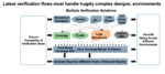
Remember the days when verification meant running a simulator with directed tests? (Back then we just called them tests.) Then came static and formal verification, simulation running in farms, emulation and FPGA prototyping. We now have UVM, constrained random testing and many different test objectives (functional, power,… Read More
One meaning of the word “reckoning” says it is the action or process of calculating or estimating something. But dead reckoning? What does that mean? Believe it or not, we have all deployed dead reckoning to varying degrees of success on different occasions. As an example, when driving on a multi-lane winding highway and direct … Read More
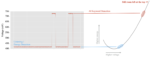
In the previous blogs on this topic, we’ve seen that utilizing near-threshold voltage (NTV) saves incredible amounts of energy, theoretically up to 10x and in practice from 2x to 4x. But there is a price which makes some applications more suited for NTV than others. This is due to the inevitable performance (speed) loss of NTV as … Read More
My first transistor-level IC design job was with Intel, doing DRAM designs by shrinking the layout to a smaller process node, and it also required running lots of SPICE runs with manually extracted parasitics to verify that everything was operating OK, meeting the access time specifications and power requirements across PVT … Read More
-Chip shortage on 60 Minutes- Average Joe now aware of chip issue
-Intel sprinkling fairy dust (money) on New Mexico & Israel
-Give up on buy backs and dividends
-Could Uncle Sam give a handout to Intel?
You normally don’t want to answer the door if 60 Minutes TV crew is outside as it likely doesn’t mean good things.… Read More


Enhancing Multi-Domain System Simulation with FMI Co-Simulation