In a power hungry world of semiconductor devices, multiple ways are being devised to budget power from system to transistor level. The success of IoT (Internet of Things) Edge devices specifically depend on lowest power, lowest area, optimal performance, and lowest cost. These devices need to be highly energy efficient for sustained battery life or longer duration. Some health care devices may not be even accessible to replace battery.
A typical SoC for tremendously growing wearable and fitness segment of IoT can have significant amount of logic, memory, and foundry IP including Flash and GPIO. The power management and wakeup circuitry on chip are essential to conserve energy during sleep mode of operation of various components or power domains. Also, energy can be minimized by optimal adjustment of Vdd and Vth at different performance levels. A key to enable successful energy saving operations in an IoT device lies in the type of Foundation IP the device employs.
There are IoT optimized low-power Foundation IP including memories and logic libraries provided by Synopsysand TSMCthat support energy saving operations by various means in SoCs. Synopsys provides TSMC sponsored 40nm ULP logic libraries for IoT applications that can be with or without eFlash. It contains power optimization kits and low-power cell kits for low voltage operations (down to 60% of VddNom) with reduced leakage and dynamic power. The power optimization kits contain special cells such as power gate, isolation cell, always-on, retention register, and level shifter to enable operations such as eliminating leakage in idle cells, managing multiple voltage domains, lowering leakage in active mode, and so on. For example, Synopsys provides an innovative ‘Live Latch’ for retention register with its protocol fully adopted in Liberty UPF and CPF systems. The TSMC sponsored offering includes different clusters of PVTs to manage power domains ranging from 0.9v +/- 10% to 1.1v +/- 10%.
There are special foundation blocks with optimized structures for low-power beyond what is provided by voltage and time based operations to reduce power. Let’s analyze a few of these.

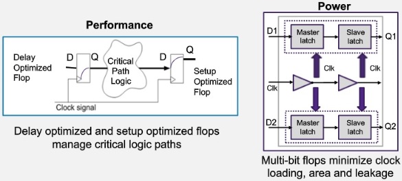
There are special FFs that can stretch performance at low voltages and minimize power. On the left side of the above picture, the delay optimized flop passes a signal very fast from clock to Q and the setup optimized flop catches the signal at very low setup time or even negative setup time, thus allowing a faster clock. On the right side, there is a 2-bit flop that operates on a single clock line. This reduces the load (capacitance) on clock line which improves area and leakage. The methodology can be used for larger flop structures, thus reducing a significant amount of power spent in a clock tree.
There is ULL (Ultra Low Leakage) library for always-on wakeup circuits that supports a wide range of voltage operations from 0.9v to 3.6v and a leakage reduction of up to 100x. The ULL control block is used to manage power of a device through on-chip LDOs (low-dropout regulators) as well as off-chip regulators. It also provides alarms to wakeup SoC, logic, memory, and so on.

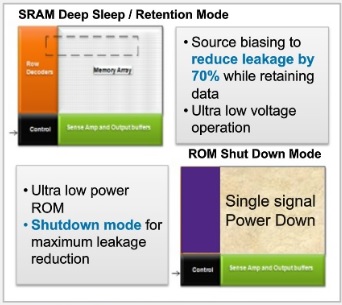
The IoT devices need high density memories with low leakage and power reduction modes. Above is an example where source biasing can be used to reduce leakage in an SRAM by 70%. There is ultra-low-power viaROM with 20%+ leakage reduction. The array can be shut down when not in use.

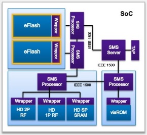
Synopsys provides a DesignWare System for embedded and external memory test, repair and diagnostics. It has very small BIST footprint. It supports SST’s 40nm eFlash. The errors in an eFlash which are different than in SRAM can be searched and the affected cells can be substituted by a column of bit cells. The system is seamlessly integrated with a Yield Accelerator and a SiliconBrowser. The award winning debug and diagnostic ecosystem allows seamless entry into the device from a PC.
Oticon designed a hearing aid device using 65LP DesignWare memory and logic IP. It runs multi-DSP core at extremely low voltages and uses power optimization kit to manage multiple voltage domains. The device is being migrated to 40nm.
With low-power foundation IP and high density eFlash which are big enablers for IoT devices, 40ULP is an attractive technology node for IoT devices as it provides a significant gain in area compared to 55nm and 90nm. TSMC 40ULP has 7-track UHD with less leakage and less power, and 9-track HD libraries for higher performance. There are various options to choose between performance and leakage from a range of libraries at 7-track UHD.
It’s important that the EDA tools and flows understand various techniques used to reduce power. For example, performance flops and multi-bit flops need to be understood by synthesis, clock-tree synthesis, P&R, DFT and verification tools.
There is a webinar sponsored by Synopsys in which Ken Brock has provided lot of details about how this ULP Foundation IP at 40nm provides an attractive solution for IoT devices. The on-line webinar is freely available HERE. It requires an instant registration.
Pawan Kumar Fangaria
Founder & President at www.fangarias.com


Comments
0 Replies to “Build Low Power IoT Design with Foundation IP at 40nm”
You must register or log in to view/post comments.