Way back in 2002 there was a study from Collett International Research on functional verification, and since 2010 the Wilson Research Group has continued that same kind of study with a new report every two years. What attracts me to this report is that it doesn’t just look at the installed base of one EDA vendor, instead it looks across the world asking questions of design and verification engineers, so that the rest of us in the semiconductor industry can understand what the trends are for functional verification.
Our global semiconductor market had a total value of $547 billion in 2021, dipping to $545 billion in 2023, then forecasted to grow to $635 billion in 2025, according to IBS, where the IC and ASIC segment would reach $330.9 billion in 2025. Systems designers using IC and ASIC components expect that functional verification has been thorough and correct, ensuring that their products operate properly and reliably.
980 engineers responded to the 2022 survey across the implementation spectrum of FPGA, IC, ASIC, full custom, structured custom, structured ASIC, to even include embedded array and gate array design styles. This blog focuses just on the IC and ASIC segments.
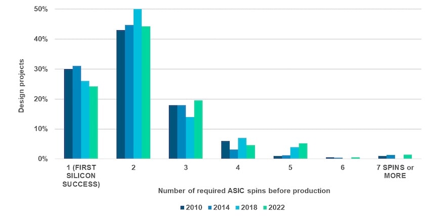
The very first metric in the report showed a sad result that first silicon success was moving downwards at only 24%, which means an expensive re-spin plus lost time to market for even more lost revenues.
The top five causes for these silicon re-spins in ranked order are:
- Logic, functional
- Analog
- Power Consumption
- Clocking
- Yield
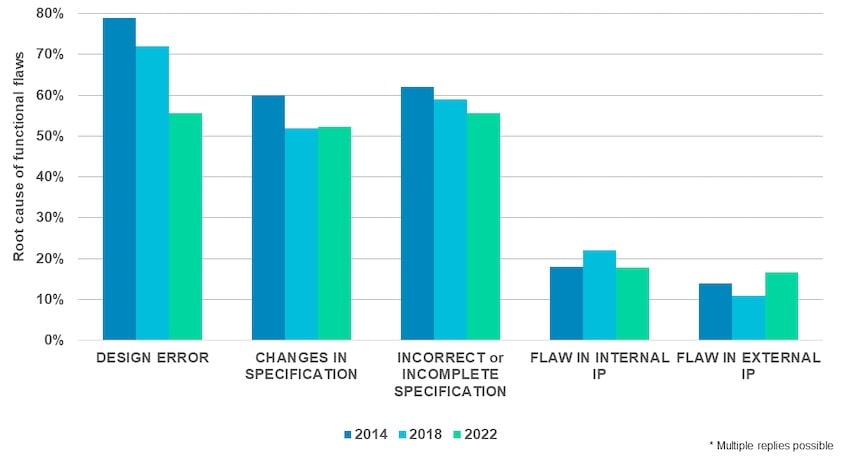
So functional flaws are the number one cause for failure, then this category is expanded to show us how design errors, changes in the specification and incorrect specification are the low-level culprits. IP vendors should note that both internal and external IP blocks contribute less to functional flaws than design errors.
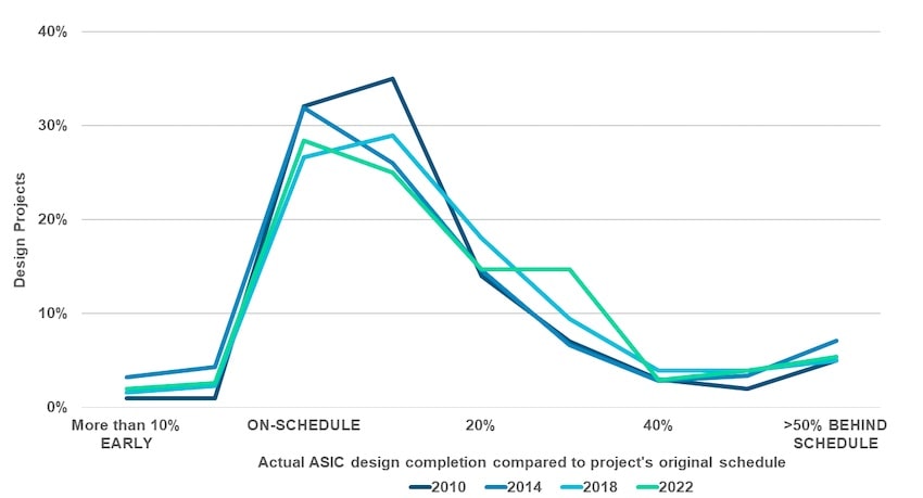
Here’s a common question from management, “Is the project on schedule?” Not quite is the realistic answer, as 66% of IC and ASIC projects completed behind schedule.
The percentage of total time spent in functional verification has held pretty constant since 2008 at about 70%, while the mean peak number of both design and verification engineers has grown to about 12. Even design engineers are spending 49% of their time doing verification. Verification engineers spread their time doing five activities:
- 47% – Test planning
- 21% – Creating Test and Running Simulation
- 15% – Testbench Development
- 13% – Debug
- 5% – Other
IC and ASIC trends show that the number of embedded processor cores is increasing, as 74% have one or more cores, 52% include two or more cores, and 15% have eight or more cores. RISC-V processors were found n 30% of designs in 2022, up 23% from two years prior. AI accelerators were seen in 32% of designs. To manage power on SoC designs we see an increase in the number of clock domains, with 3-4 being the average number.
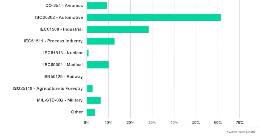
Asynchronous clock domains are predominant at 93% of designs, creating a need for more gate-level simulation and CDC verification tools. Security features are being added to 58% of IC/ASIC designs for things like encryption keys, DRM keys and handling sensitive data. Here’s the distribution for safety-critical standards:
FuSa (Functional Safety) project time was spent on four activities, taking less than 25% of project time: Safety Analysis, Safety Architecture and design, Safety requirements, Safety verification.
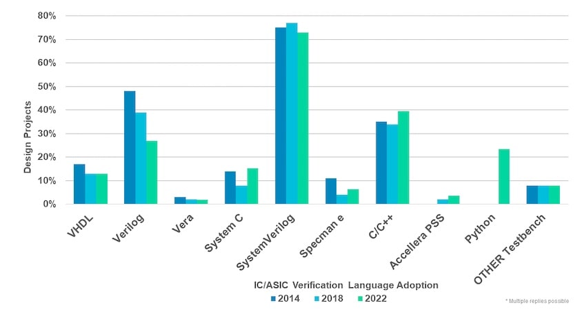
Verification languages and methodology are spread out across 10 categories, with SystemVerilog in top use, while Verilog use decreases, and Python is an emerging trend:
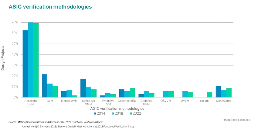
Accellera UVM remains the most used verification methodology, and the Python-based cocotb was recently added this year.
For assertion languages there is SystemVerilog Assertions still on top at 72%, with OVL at 15% and PSL at 9%. Formal property checking was used in 35% of designs, and automatic formal checking grew to 32% of designs, both categories grew quickly in the past 8 years.
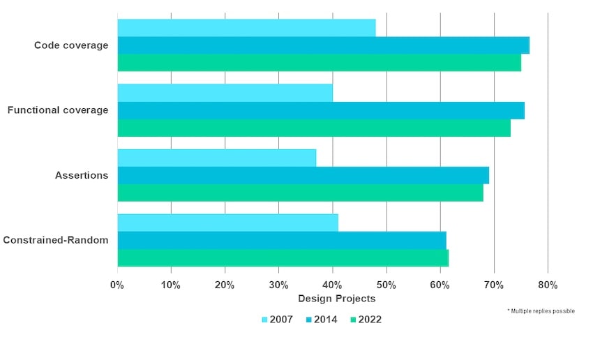
There are four simulation-based techniques tracked in the survey, so no new approaches added in the past 15 years:
Software-based verification is limited by speed and capacity issues, so hardware-based emulation and FPGA prototyping have arrived just in time to help verify the largest SoC devices by running actual software and operating systems. The top six reasons to use emulation or FPGA prototyping are listed with HW/SW co-design and verification as the most important factor.
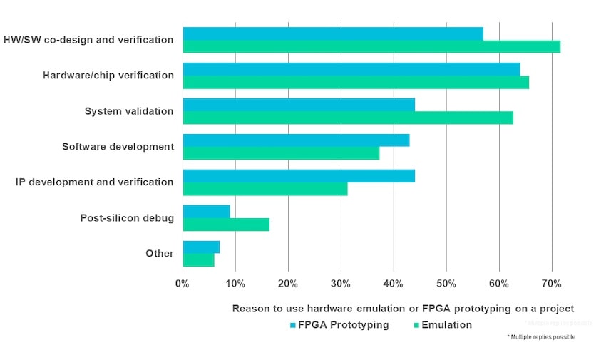
Emulation and prototyping have recently improved in capacity to exceed 1 billion gates, not counting memories.
Summary
Functional verification is essential to knowing that a new electronic design meets the specification, functions reliably and works properly on first silicon. Both design and verification engineers spend their time in functional verification using multiple languages, methodologies and even hardware-assisted platforms to reach their goals of on-time project delivery. This bi-annual report is rich with information to help our industry see the functional trends for IC and ASIC designers, then respond with best practices and keep engineers updated and trained on how to work smarter, not harder.
Read the complete 17 page report by requesting it online.
Stay tuned for a separate blog on FPGA functional verification trends.
Related Blogs
- Achieving Faster Design Verification Closure
- An Update on HLS and HLV
- Connecting SystemC to SystemVerilog
- Today’s SoC Design Verification and Validation Require Three Types of Hardware-Assisted Engines
- Verifying 10+ Billion-Gate Designs Requires Distinct, Scalable Hardware Emulation Architecture
- UVM Polymorphism is Your Friend
- Coverage Analysis in Questa Visualizer
- EDA in the Cloud with Siemens EDA at #59DAC
Share this post via:


Comments
There are no comments yet.
You must register or log in to view/post comments.